background image

CC1150

www.ti.com

SWRS037B – JANUARY 2006 – REVISED MARCH 2015

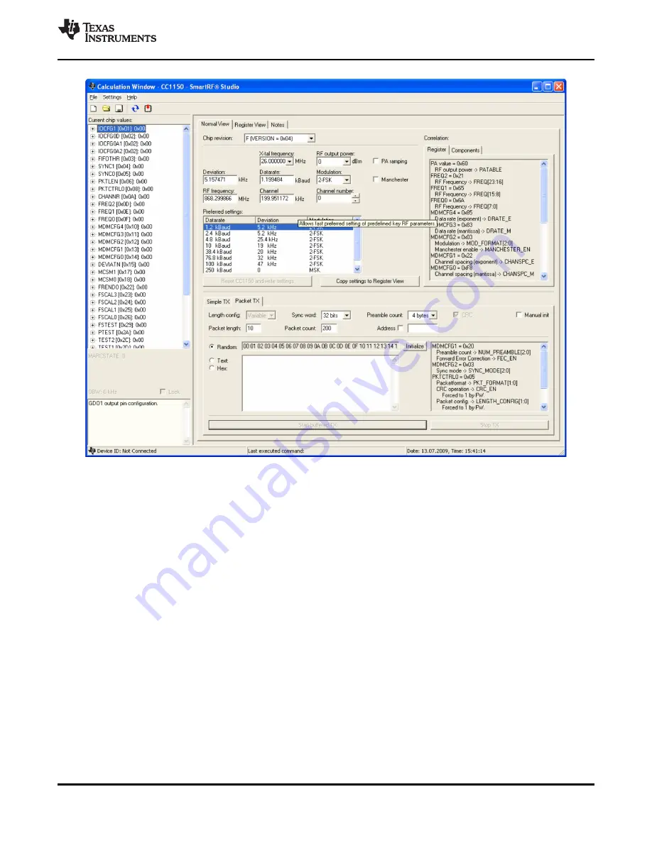
Figure 5-3. SmartRF Studio User Interface

5.5

4-wire Serial Configuration and Data Interface

CC1150 is configured via a simple 4-wire SPI-compatible interface (SI, SO, SCLK and CSn) where
CC1150 is the slave. This interface is also used to read and write buffered data. All address and data
transfer on the SPI interface is done most significant bit first.

All transactions on the SPI interface start with a header byte containing a read/write bit, a burst access bit
and a 6-bit address.

During address and data transfer, the CSn pin (Chip Select, active low) must be kept low. If CSn goes
high during the access, the transfer will be cancelled. The timing for the address and data transfer on the
SPI interface is shown in

Figure 5-4

with reference to

Table 5-1

.

When CSn is pulled low, the MCU must wait until the CC1150 SO pin goes low before starting to transfer
the header byte. This indicates that the voltage regulator has stabilized and the crystal is running. Unless
the chip is in the SLEEP or XOFF states, the SO pin will always go low immediately after taking CSn low.

Copyright © 2006–2015, Texas Instruments Incorporated

Detailed Description

13

Submit Documentation Feedback

Product Folder Links:

CC1150

Summary of Contents for CC1150

Page 1: ...dio Communication Protocols Optional Forward Error Correction with Interleaving 1 2 Applications Ultra low Power UHF Wireless Transmitters Low Power Telemetry Operating in the 315 433 868 and 915 MHz Home and Building Automation ISM SRD bands Wireless Alarm and Security Systems AMR Automatic Meter Reading Industrial Monitoring and Control Consumer Electronics Wireless Sensor Networks RKE Remote Ke...

Page 2: ...SWRS037B JANUARY 2006 REVISED MARCH 2015 www ti com Table 1 1 Device Information 1 PART NUMBER PACKAGE BODY SIZE CC1150 VQFNP 16 4 00 mm 4 00 mm 1 For more information see Section 8 Mechanical Packaging and Orderable Information 1 4 Functional Block Diagram 2 Device Overview Copyright 2006 2015 Texas Instruments Incorporated Submit Documentation Feedback Product Folder Links CC1150 ...

Page 3: ...Current Consumption 7 5 20 Memory 38 4 6 RF Transmit 7 6 Applications Implementation and Layout 51 4 7 Crystal Oscillator 8 6 1 Application Information 51 4 8 Frequency Synthesizer Characteristics 8 6 2 Design Requirements 53 4 9 Analog Temperature Sensor 9 6 3 PCB Layout Recommendations 55 4 10 DC Characteristics 9 7 Device and Documentation Support 58 4 11 Power On Reset 10 7 1 Device Support 58...

Page 4: ...highlights the changes made to the SWRS037A device specific data manual to make it an SWRS037B revision Changes from January 1 2006 to February 19 2015 Page Updated RST package to RGV 58 4 Revision History Copyright 2006 2015 Texas Instruments Incorporated Submit Documentation Feedback Product Folder Links CC1150 ...

Page 5: ... XOSC_Q2 Analog I O Crystal oscillator pin 2 Digital output pin for general use Test signals GDO0 FIFO status signals 8 Digital I O ATEST Clock output down divided from XOSC Serial input TX data Also used as analog test I O for prototype production testing 9 CSn Digital Input Serial configuration interface chip select 10 RF_P RF I O Positive RF output signal from PA 11 RF_N RF I O Negative RF outp...

Page 6: ...s VALUE UNIT Human body model HBM per ANSI ESDA JEDEC JS 001 1 2 500 V ESD Electrostatic discharge V Charged device model CDM 250 1 JEDEC document JEP155 states that 500 V HBM allows safe manufacturing with a standard ESD control process Manufacturing with less than 500 V HBM is possible with the necessary precautions 2 According to JEDEC STD 22 method A114 Human Body Model 4 3 Recommended Operati...

Page 7: ... DN012 3 29 3 mA Transmit mode 10 dBm output power 0xC0 Current consumption 915 MHz 15 2 mA Transmit mode 0 dBm output power 0x50 See more in Section 5 16 and DN012 3 4 6 RF Transmit Tc 25 C VDD 3 0 V if nothing else stated All measurement results are obtained using the CC1150EM reference design see 1 and 2 PARAMETER TYP MAX UNIT CONDITION 315 MHz 122 j31 Ω Differential impedance as seen from the ...

Page 8: ... 3 0 V if nothing else is stated All measurement results obtained using the CC1150EM reference design see 1 and 2 PARAMETER MIN TYP MAX UNIT CONDITION Crystal frequency 26 26 27 MHz This is the total tolerance including a initial tolerance b aging and c temperature dependence Tolerance 40 ppm The acceptable crystal tolerance depends on RF frequency and channel spacing bandwidth Load capacitance 10...

Page 9: ...27 26 26 MHz crystal 694 721 721 µs frequency 4 9 Analog Temperature Sensor 1 Tc 25 C VDD 3 0 V if nothing else is stated PARAMETER MIN TYP MAX UNIT CONDITION Output voltage at 40 C 0 651 V Output voltage at 0 C 0 747 V Output voltage at 40 C 0 847 V Output voltage at 80 C 0 945 V Temperature coefficient 2 45 mV C Fitted from 20 C to 80 C From 20 C to 80 C when using Absolute error in calculated t...

Page 10: ...ction to package top 1 6 PsiJB Junction to board 25 2 RθJC bottom Junction to case bottom 6 3 1 C W degrees Celsius per watt 2 These values are based on a JEDEC defined 2S2P system with the exception of the Theta JC RθJC value which is based on a JEDEC defined 1S0P system and will change based on environment as well as application For more information see these EIA JEDEC standards JESD51 2 Integra...

Page 11: ...am Figure 5 1 CC1150 Simplified Block Diagram 5 3 Configuration Overview CC1150 can be configured to achieve optimum performance for many different applications Configuration is done using the SPI interface The following key parameters can be programmed Power down and power up mode Crystal oscillator power up and power down Transmit mode RF channel selection Data rate Modulation format RF output p...

Page 12: ... mA Typ current consumption 868 MHz 14 mA at 10 dBm output 15 mA at 0 dBm output 24 mA at 7 dBm output 29 mA at 10 dBm output Optional transitional state Typ current consumption 7 7 mA In FIFO based modes transmission is turned off and this state entered if the TX FIFO becomes empty in the middle of a packet Typ current consumption 1 1 mA CC1150 SWRS037B JANUARY 2006 REVISED MARCH 2015 www ti com ...

Page 13: ...6 bit address During address and data transfer the CSn pin Chip Select active low must be kept low If CSn goes high during the access the transfer will be cancelled The timing for the address and data transfer on the SPI interface is shown in Figure 5 4 with reference to Table 5 1 When CSn is pulled low the MCU must wait until the CC1150 SO pin goes low before starting to transfer the header byte ...

Page 14: ...a bytes and Burst access 76 ns between data bytes thd Hold data after positive edge on SCLK 20 ns tns Negative edge on SCLK to CSn high 20 ns NOTE The minimum tsp pd figure in Table 5 1 can be used in cases where the user does not read the CHIP_RDYn signal CSn low to positive edge on SCLK when the chip is woken from power down depends on the start up time of the crystal being used The 150 μs in Ta...

Page 15: ... is transmitted on the SI pin When reading from registers the status byte is sent on the SO pin each time a header byte is transmitted on the SI pin Registers with consecutive addresses can be accessed in an efficient way by setting the burst bit in the address header The address sets the start address in an internal address counter This counter is incremented by one each new byte every 8 clock pu...

Page 16: ...he TX FIFO is write only The burst bit is used to determine if FIFO access is single byte or a burst access The single byte access method expects address with burst bit set to zero and one data byte After the data byte a new address is expected hence CSn can remain low The burst access method expects one address byte and then consecutive data bytes until terminating the access by setting CSn high ...

Page 17: ... highest 7 one byte at a time An index counter is used to control the access to the table This counter is incremented each time a byte is read or written to the table and set to the lowest index when CSn is high When the highest value is reached the counter restarts at zero The access to the PATABLE is either single byte or burst access depending on the burst bit When using burst access the index ...

Page 18: ... Optional Radio Control Feature The CC1150 has an optional way of controlling the radio by reusing SI SCLK and CSn from the SPI interface This feature allows for a simple three pin control of the major states of the radio SLEEP IDLE and TX This optional functionality is enabled with the MCSM0 PIN_CTRL_EN configuration bit State changes are commanded as follows If CSn is high the SI and SCLK are se...

Page 19: ... the following elements to the packet stored in the TX FIFO A programmable number of preamble bytes A two byte Synchronization Word Can be duplicated to give a 4 byte sync word recommended It is not possible to only insert preamble or only insert a sync word Optionally whitening the data with a PN9 sequence Optionally Interleave and Forward Error Code the data Optionally compute and add a 2 byte C...

Page 20: ...ta before transmitting and de whitening in the receiver With CC1150 in combination with a CC1101 at the receiver end this can be done automatically by setting PKTCTRL0WHITE_DATA 1 All data except the preamble and the sync word are then XOR ed with a 9 bit pseudo random PN9 sequence before being transmitted as shown in Figure 5 7 The PN9 sequence is initialized to all ones At the receiver end the d...

Page 21: ...length is set to infinite and transmission will continue until turned off manually The infinite mode can be turned off while a packet is being transmitted As described in Section 5 8 2 1 this can be used to support packet formats with different length configuration than natively supported by CC1150 One should make sure that TX mode is not turned off during the transmission of the first half of any...

Page 22: ...d This is done before the optional FEC Interleaver stage Whitening is enabled by setting PKTCTRL0 WHITE_DATA 1 If FEC Interleaving is enabled the length byte payload data and the two CRC bytes will be scrambled by the interleaver and FEC encoded before being modulated FEC is enabled by setting MDMCFG1 FEC_EN 1 5 8 4 Packet Handling in Firmware When implementing a packet oriented radio protocol in ...

Page 23: ...ure improves adjacent channel power ACP and occupied bandwidth In true 2 FSK systems with abrupt frequency shifting the spectrum is inherently broad By making the frequency shift softer the spectrum can be made significantly narrower Thus higher data rates can be transmitted in the same bandwidth using GFSK The frequency deviation is programmed with the DEVIATION_M and DEVIATION_E values in the DE...

Page 24: ... of some bit errors The use of FEC allows correct reception at a lower Signal to Noise RATIO SNR thus extending communication range Alternatively for a given SNR using FEC decreases the bit error rate BER As the packet error rate PER is related to BER by Equation 4 PER 1 1 BER packet_length 4 A lower BER can be used to allow longer packets or a higher percentage of packets of a given length to be ...

Page 25: ...f the matrix and fed to the rate convolutional coder Conversely in a CC1101 receiver the received symbols are written into the rows of the matrix whereas the data passed onto the convolutional decoder is read from the columns of the matrix When FEC and interleaving is used at least one extra byte is required for trellis termination In addition the amount of data transmitted over the air must be a ...

Page 26: ...BRATE 12 IDLE 1 TXOFF_MODE 00 FS_AUTOCAL 10 11 TXOFF_MODE 00 FS_AUTOCAL 00 01 TXOFF_MODE 10 FS_WAKEUP 6 7 STX SFSTXON SLEEP 0 SPWD XOFF 2 SXOFF CSn 0 CSn 0 TXOFF_MODE 01 CC1150 SWRS037B JANUARY 2006 REVISED MARCH 2015 www ti com 5 11 Radio Control Figure 5 11 Radio Control State Diagram 26 Detailed Description Copyright 2006 2015 Texas Instruments Incorporated Submit Documentation Feedback Product...

Page 27: ...nimum requirements stated in Section 4 7 must be followed for the power on reset to function properly The internal power up sequence is completed when CHIP_RDYn goes low CHIP_RDYn is observed on the SO pin after CSn is pulled low See Section 10 1 for more details on CHIP_RDYn When the CC1150 reset is completed the chip will be in the IDLE state and the crystal oscillator running If the chip has ha...

Page 28: ...the crystal oscillator can be found in Section 4 7 5 11 3 Voltage Regulator Control The voltage regulator to the digital core is controlled by the radio controller When the chip enters the SLEEP state which is the state with the lowest current consumption the voltage regulator is disabled This occurs after CSn is released when a SPWD command strobe has been sent on the SPI interface The chip is th...

Page 29: ... XOSC start up times are variable but within the limits stated in Section 4 7 NOTE In a frequency hopping spread spectrum or a multi channel protocol the calibration time can be reduced from 721 µs to approximately 150 µs This is explained in Section 5 19 2 Table 5 6 State Transition Timing DESCRIPTION XOSC PERIODS 26 MHz CRYSTAL Idle to TX FSTXON no calibration 2298 88 4 µs Idle to TX FSTXON with...

Page 30: ...t FIFOTHR FIFO_THR setting is used to program the FIFO threshold point Table 5 7 lists the 16 FIFO_THR settings and the corresponding thresholds for the TX FIFO Figure 5 14 Example of FIFO at Threshold A flag will assert when the number of bytes in the FIFO is equal to or higher than the programmed threshold The flag is used to generate the FIFO status signals that can be viewed on the GDO pins se...

Page 31: ...teristics will vary with temperature and supply voltage changes as well as the desired operating frequency In order to ensure reliable operation CC1150 includes frequency synthesizer self calibration circuitry This calibration should be done regularly and must be performed after turning on power and before using a new frequency or channel The number of XOSC cycles for completing the PLL calibratio...

Page 32: ...ne external decoupling capacitor The voltage regulator output should only be used for driving the CC1150 5 16 Output Power Programming The RF output power level from the device has two levels of programmability as illustrated in Figure 5 16 Firstly the special PATABLE register can hold up to eight user selected output power settings Secondly the 3 bit FREND0 PA_POWER value selects the PATABLE entr...

Page 33: ...ASK modulation up to eight power settings are used for shaping The modulator contains a counter that counts up when transmitting a one and down when transmitting a zero The counter counts at a rate equal to 8 times the symbol rate The counter saturates at FREND0 PA_POWER and 0 respectively This counter value is used as an index for a lookup in the power table Thus in order to utilize the whole tab...

Page 34: ...rved defined on the transceiver version CC1101 9 0x09 Reserved defined on the transceiver version CC1101 Lock detector output The PLL is in lock if the lock detector output has a positive transition or is constantly 10 0x0A logic high To check for PLL lock the lock detector output should be used as an interrupt for the MCU Serial Clock Synchronous to the data in synchronous serial mode 11 0x0B In ...

Page 35: ...efault value is CLK_XOSC 192 2 To optimize RF performance these signals should not be used while the radio is in TX mode 5 18 Asynchronous and Synchronous Serial Operation Several features and modes of operation have been included in the CC1150 to provide backward compatibility with previous TI products and other existing RF communication systems For new systems it is recommended to use the built ...

Page 36: ...in the 315 MHz 433 MHz 868 MHz or 915 MHz frequency bands The CC1150 is specifically designed for such use with its 300 to 348 MHz 400 to 464 MHz and 800 to 928 MHz operating ranges The most important regulations when using the CC1150 in the 315 MHz 433 MHz 868 MHz or 915 MHz frequency bands are EN 300 220 Europe and FCC CFR47 part 15 USA A summary of the most important aspects of these regulation...

Page 37: ...one should always use SmartRF Studio 11 to get the correct settings for a specific frequency before doing a calibration regardless of which calibration method is being used It must be noted that the content of the CC1150 is not retained in SLEEP state and thus it is necessary to write to the TEST0 register along with other registers when returning from the SLEEP state and initiating calibrations 5...

Page 38: ...tem parameters are most easily found by using the SmartRF Studio 11 software Complete descriptions of the registers are given in Section 5 20 1 After chip reset all the registers have default values as shown in the tables The optimum register setting might differ from the default value After a reset all registers that shall be different from the default value therefore needs to be programmed throu...

Page 39: ...SNOP No operation May be used to pad strobe commands to two bytes for simpler software Table 5 12 Configuration Registers Overview ADDRESS ACRONYM REGISTER NAME SECTION 0x01 IOCFG1 GDO1 output pin configuration Table 5 14 0x02 IOCFG0 GDO0 output pin configuration Table 5 15 0x03 FIFOTHR FIFO threshold Table 5 16 0x04 SYNC1 Sync word high byte Table 5 17 0x05 SYNC0 Sync word low byte Table 5 18 0x0...

Page 40: ... 5 40 0x2C TEST2 Various test settings Table 5 41 0x2D TEST1 Various test settings Table 5 42 0x2E TEST0 Various test settings Table 5 43 Table 5 13 Status Registers Overview ADDRESS ACRONYM REGISTER NAME SECTION 0x30 0xF0 PARTNUM Part number for CC1150 Table 5 44 0x31 0xF1 VERSION Current version number Table 5 45 0x35 0xF5 MARCSTATE Control state machine state Table 5 46 0x38 0xF8 PKTSTATUS Curr...

Page 41: ... 0x2A PTEST 0x2B AGCTEST 0x2C TEST2 0x2D TEST1 0x2E TEST0 0x2F 0x30 SRES SRES PARTNUM Command Strobes Status registers read only and multi byte registers 0x31 SFSTXON SFSTXON VERSION 0x32 SXOFF SXOFF FREQEST 0x33 SCAL SCAL LQI 0x34 SRX SRX RSSI 0x35 STX STX MARCSTATE 0x36 SIDLE SIDLE WORTIME1 0x37 SAFC SAFC WORTIME0 0x38 SWOR SWOR PKTSTATUS 0x39 SPWD SPWD VCO_VC_DAC 0x3A SFRX SFRX TXBYTES 0x3B SFT...

Page 42: ...tialization in order to optimize RF performance Table 5 16 0x03 FIFOTHR FIFO Threshold BIT FIELD TYPE RESET DESCRIPTION 7 4 Reserved R W 0x0 Write 0 for compatibility with possible future extensions 3 0 FIFO_THR 3 0 R W 0x07 Set the threshold for the TX FIFO The threshold is exceeded when the number of bytes in the FIFO is equal to or higher than the threshold value The binary number is the settin...

Page 43: ...ransparent mode Data in on GDO0 3 R W 0x0 Not used 2 CRC_EN R W 0x1 1 CRC calculation enabled 0 CRC disabled 1 0 LENGTH_CONFIG 1 0 R W 0x1 Configure the packet length The binary number is the setting and the result is the packet length configuration 00 Fixed length packets length configured in PKTLEN register 01 Variable length packets packet length configured by the first byte after sync word 10 ...

Page 44: ...te BIT FIELD TYPE RESET DESCRIPTION 7 0 FREQ 7 0 R W 0xEC Ref FREQ2 register Table 5 26 0x10 MDMCFG4 Modulator Configuration BIT FIELD TYPE RESET DESCRIPTION 7 4 Reserved R0 0x08 Defined on the transceiver version CC1101 3 0 DRATE_E 3 0 R W 0x0C The exponent of the user specified symbol rate Table 5 27 0x11 MDMCFG3 Modulator Configuration BIT FIELD TYPE RESET DESCRIPTION 7 0 DRATE_M 7 0 R W 0x22 T...

Page 45: ...e setting and the result is the Sync word qualifier mode for compatibility with the CC1101 transceiver 000 No preamble sync word 001 15 16 sync word bits detected 010 16 16 sync word bits detected 011 30 32 sync word bits detected 100 No preamble sync carrier sense above threshold 101 15 16 carrier sense above threshold 110 16 16 carrier sense above threshold 111 30 32 carrier sense above threshol...

Page 46: ... during which a phase change occurs 0 90deg 1 90deg Refer to the SmartRF Studio 11 software for correct DEVIATN setting when using MSK When 2 FSK GFSK modulation is enabled Deviation mantissa interpreted as a 4 bit value with MSB implicit 1 The resulting frequency deviation is given by Equation 9 9 The default values give 47 607 kHz deviation assuming 26 0 MHz crystal frequency When ASK OOK modula...

Page 47: ...timeout after XOSC start 00 1 Approx 2 3 μs 2 7 μs 01 16 Approx 37 μs 43 μs 10 64 Approx 146 μs 171 μs 11 256 Approx 585 μs 683 μs Exact timeout depends on crystal frequency In order to reduce start up time from the SLEEP state this field is preserved in powerdown SLEEP state 1 0 Reserved R0 Defined on the transceiver version CC1101 Table 5 34 0x22 FREND0 Front End TX Configuration BIT FIELD TYPE ...

Page 48: ...t calibration for each hop can be done by calibrating up front for each frequency and saving the resulting FSCAL3 FSCAL2 and FSCAL1 register values Between each frequency hop calibration can be replaced by writing the FSCAL3 FSCAL2 and FSCAL1 register values corresponding to the next RF frequency Table 5 37 0x25 FSCAL1 Frequency Synthesizer Calibration BIT FIELD TYPE RESET DESCRIPTION 7 6 R0 Not U...

Page 49: ...s given by the SmartRF Studio 11 software Table 5 43 0x2E TEST0 Various Test Settings BIT FIELD TYPE RESET DESCRIPTION 7 2 TEST0 7 2 R W 0x02 The value to use in this register is given by the SmartRF Studio 11 software 1 VCO_SEL_CAL_EN R W 0x1 Enable VCO selection calibration stage when 1 The value to use in this register is given by the SmartRF Studio 11 software 0 TEST0 0 R W 0x1 The value to us...

Page 50: ...OFF state numbers because setting CSn low will make the chip enter the IDLE mode from the SLEEP or XOFF states 2 State see Figure 5 11 Table 5 47 0x38 0xF8 PKTSTATUS Current GDOx Status BIT FIELD TYPE RESET DESCRIPTION 7 2 Reserved R0 Defined on the transceiver version CC1101 1 R0 Not Used 0 GDO0 R Current GDO0 value Note the reading gives the non inverted value irrespective what IOCFG0 GDO0_INV i...

Page 51: ...mers are responsible for determining suitability of components for their purposes Customers should validate and test their design implementation to confirm system functionality 6 1 Application Information 6 1 1 Typical Application A simplified block diagram of CC1150 is shown in Figure 5 1 Only a few external components are required for using the CC1150 The recommended application circuits are sho...

Page 52: ...ors C101 C111 RF balun matching capacitors C102 RF LC filter matching filter capacitor 315 and 433 MHz RF balun matching capacitor 868 915 MHz C103 RF LC filter matching capacitors C104 RF balun DC blocking capacitor C105 RF LC filter DC blocking capacitor and part of optional RF LC filter 868 915 MHz C106 Part of optional RF LC filter and DC Block 868 915 MHz L101 L111 RF balun matching inductors...

Page 53: ...1 Murata LQG15HS and GRM1555C series inductors and capacitors resistor from the Koa RK73 series and AT 41CD2 crystal from NDK 6 2 Design Requirements 6 2 1 Bias Resistor The bias resistor R141 is used to set an accurate bias current 6 2 2 Balun and RF Matching The components between the RF_N RF_P pins and the point where the two signals are joined together C111 C101 L101 and L111 for the 315 433 M...

Page 54: ...own in Figure 6 3 Typical component values for different values of CL are given in Table 6 3 Figure 6 3 Crystal Oscillator Circuit The crystal oscillator is amplitude regulated This means that a high current is used to start up the oscillations When the amplitude builds up the current is reduced to what is necessary to maintain approximately 0 4 Vpp signal swing This ensures a fast start up and ke...

Page 55: ... application circuit The placement and the size of the decoupling capacitors are very important to achieve the optimum performance The CC1150EM reference design should be followed closely see 1 and 2 6 3 PCB Layout Recommendations The top layer should be used for signal routing and the open areas should be filled with metallization connected to ground using several vias The area under the chip is ...

Page 56: ... small as possible 0402 is recommended and surface mount devices are highly recommended Please note that components smaller than those specified may have differing characteristics Precaution should be used when placing the microcontroller in order to avoid noise interfering with the RF circuitry It is strongly advised that the CC1150EM reference design see 1 and 2 layout is followed very closely i...

Page 57: ...ure 6 5 is an illustration only and not to scale There are five 10 mil diameter via holes distributed symmetrically in the ground pad under the package See also the CC1150EM reference design 1 and 2 Copyright 2006 2015 Texas Instruments Incorporated Applications Implementation and Layout 57 Submit Documentation Feedback Product Folder Links CC1150 ...

Page 58: ... nomenclature also includes a suffix with the device family name This suffix indicates the package type for example RGV For orderable part numbers of CC1150 devices in the RGV package types see the Package Option Addendum of this document the TI website www ti com or contact your TI sales representative 7 2 Documentation Support The following documents describe the CC1150 device Copies of these do...

Page 59: ...ifications 7 5 Export Control Notice Recipient agrees to not knowingly export or re export directly or indirectly any product or technical data as defined by the U S EU and other Export Administration Regulations including software or any controlled product restricted by other applicable national regulations received from disclosing party under nondisclosure obligations if any or any direct produc...

Page 60: ...logen requirements of 1000ppm threshold Antimony trioxide based flame retardants must also meet the 1000ppm threshold requirement 3 MSL Peak Temp The Moisture Sensitivity Level rating according to the JEDEC industry standard classifications and peak solder temperature 4 There may be additional marking which relates to the logo the lot trace code information or the environmental category on the dev...

Page 61: ...PACKAGE OPTION ADDENDUM www ti com 30 May 2018 Addendum Page 2 ...

Page 62: ...ng Pins SPQ Reel Diameter mm Reel Width W1 mm A0 mm B0 mm K0 mm P1 mm W mm Pin1 Quadrant CC1150RGVR VQFN RGV 16 2500 330 0 12 4 4 3 4 3 1 5 8 0 12 0 Q2 CC1150RGVT VQFN RGV 16 250 180 0 12 4 4 3 4 3 1 5 8 0 12 0 Q2 PACKAGE MATERIALS INFORMATION www ti com 21 Nov 2016 Pack Materials Page 1 ...

Page 63: ...ce Package Type Package Drawing Pins SPQ Length mm Width mm Height mm CC1150RGVR VQFN RGV 16 2500 336 6 336 6 28 6 CC1150RGVT VQFN RGV 16 250 210 0 185 0 35 0 PACKAGE MATERIALS INFORMATION www ti com 21 Nov 2016 Pack Materials Page 2 ...

Page 64: ......

Page 65: ......

Page 66: ...oduct s identified in such TI Resource NO OTHER LICENSE EXPRESS OR IMPLIED BY ESTOPPEL OR OTHERWISE TO ANY OTHER TI INTELLECTUAL PROPERTY RIGHT AND NO LICENSE TO ANY TECHNOLOGY OR INTELLECTUAL PROPERTY RIGHT OF TI OR ANY THIRD PARTY IS GRANTED HEREIN including but not limited to any patent right copyright mask work right or other intellectual property right relating to any combination machine or p...

Reviews: