background image

Chapter 2: Installation

2-5

Top View of DIMM Slot

R e l e a s e   T a b

R e l e a s e   T a b

To Remove:
Use your thumbs to gently push each release tab outward.
This should release the DIMM from the slot.

2-5

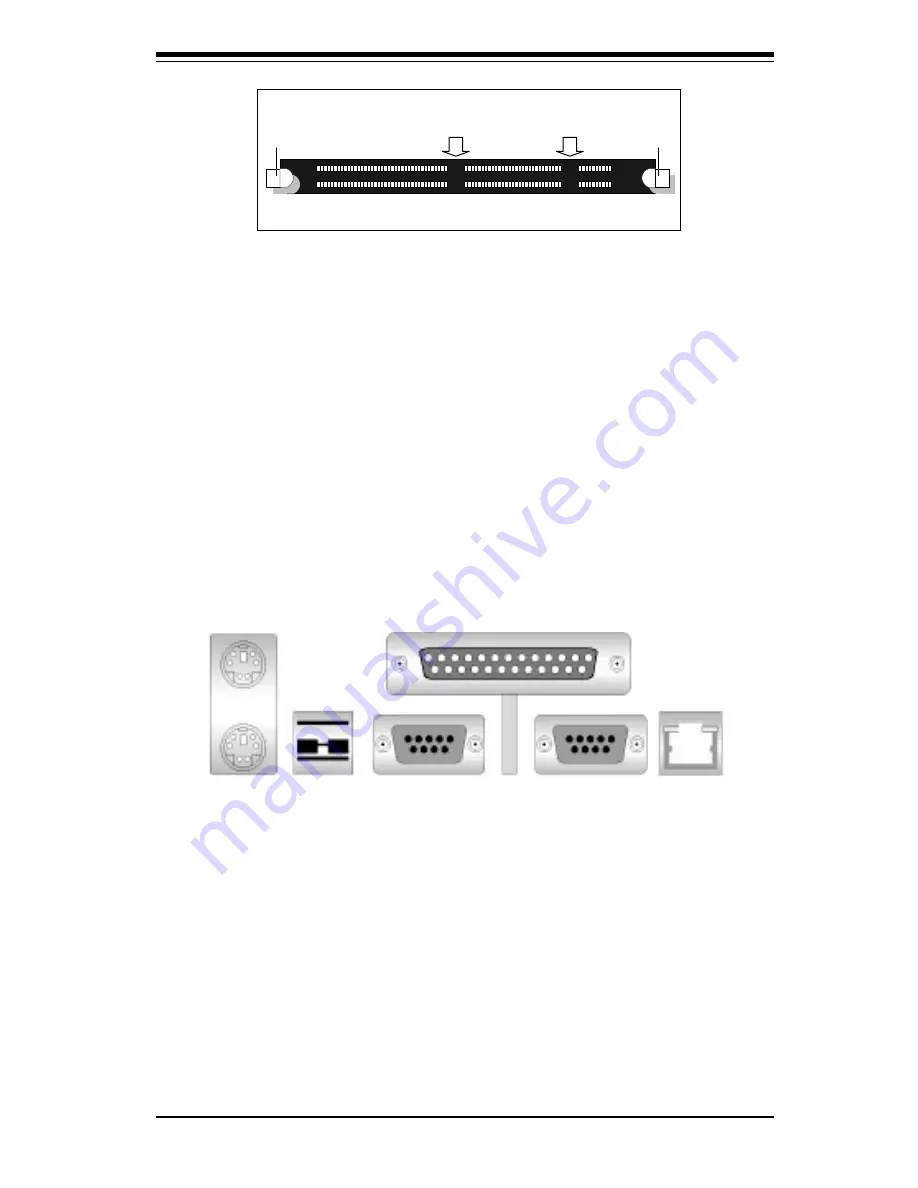
Port/Control Panel Connector Locations

The I/O ports are color coded in conformance with the PC 99 specification.

See Figure 2-5 below for the colors and locations of the various I/O ports.

Figure 2-5.  I/O Port Locations and Definitions

Parallel Port

 (Burgundy)

 COM1                   COM2

Keyboard

(Purple)

Mouse

(Green)

Ethernet

  Port

(Black)

       (Turquoise)

USB

Ports

(Black)

Summary of Contents for SUPER P3TDL3

Page 1: ...SUPER P3TDL3 SUPER P3TDLE USER S MANUAL Revision 1 0c SUPER...

Page 2: ...ILITY TO USE THIS PRODUCT OR DOCUMENTATION EVEN IF ADVISED OF THE POSSIBILITY OF SUCH DAMAGES IN PARTICULAR THE VENDOR SHALL NOT HAVE LIABILITY FOR ANY HARDWARE SOFTWARE OR DATA STORED OR USED WITH TH...

Page 3: ...on handling static sensitive devices Read this chapter when you want to install the processor and DIMM memory modules and when mounting the mainboard in the chassis Also refer to this chapter to conne...

Page 4: ...atures of the P3TDL3 P3TDLE Motherboard 1 11 1 2 Chipset Overview 1 12 1 3 Special Features 1 13 BIOS Recovery 1 13 Recovery from AC Power Loss 1 13 1 4 PC Health Monitoring 1 14 1 5 ACPI PC 98 Featur...

Page 5: ...dicator 2 12 Ethernet Port 2 13 Serial Ports 2 13 ATX PS 2 Keyboard and Mouse Ports 2 13 2 7 DIP Switch Settings 2 14 DIP Switch 1 Core Bus Ratio 2 14 2 8 Jumper Settings 2 15 CMOS Clear 2 15 SCSI Ter...

Page 6: ...equently Asked Questions 3 3 3 4 Returning Merchandise for Service 3 5 Chapter 4 BIOS 4 1 Introduction 4 1 4 2 BIOS Features 4 2 4 3 Running Setup 4 2 Main BIOS Setup Menu 4 3 4 4 Advanced BIOS Setup...

Page 7: ...all been included with your motherboard If anything listed here is damaged or missing contact your retailer One 1 Supermicro Mainboard One 1 ribbon cable for IDE devices One 1 floppy ribbon cable for...

Page 8: ...ope Address SuperMicro Computer B V Het Sterrenbeeld 28 5215 ML s Hertogenbosch The Netherlands Tel 31 0 73 6400390 Fax 31 0 73 6416525 Email sales supermicro nl General Information support supermicro...

Page 9: ...Chapter 1 Introduction 1 3 Introduction Notes...

Page 10: ...SUPER P3TDL3 P3TDLE User s Manual 1 4 Introduction SUPER P3TDL3 Figure 1 1 SUPER P3TDL3 Image...

Page 11: ...Chapter 1 Introduction 1 5 Introduction SUPER P3TDLE Figure 1 2 SUPER P3TDLE...

Page 12: ...104 Ethernet Port FCPGA Processor 1 FCPGA Processor 2 North Bridge DIMM2 DIMM3 DIMM0 DIMM1 IDE 1 IDE 2 ULTRA WIDE SCSI PWR_SEC JP12 JF1 J24 JP2 JA4 JP1 JP11 JP7 PCI 3 Thermal Fan ULTRA SCSI FLOPPY USB...

Page 13: ...us Ratio See Section 2 7 Connectors Description Chassis Fan 4 7 Chassis Fan Headers COM1 2 COM1 COM2 Serial Port Connector CPU FAN 1 2 CPU1 CPU2 Fan Header DIMM0 DIMM3 Memory RAM Slots J23 J24 IDE Har...

Page 14: ...MM3 DIMM0 DIMM1 IDE 1 IDE 2 PWR_SEC JP12 JF1 J24 JP2 JP11 JP7 PCI 3 Thermal Fan FLOPPY USB4 PCI 4 PCI 2 PCI 1 PCI 64 2 PCI 64 1 ISA South Bridge AIC 7892 Super I O BIOS Battery 24 PIN ATX POWER U45 JP...

Page 15: ...tion Default Setting SW1 1 4 CPU Core Bus Ratio See Section 2 7 Connectors Description Chassis Fan 4 7 Chassis Fan Headers COM1 2 COM1 COM2 Serial Port Connector CPU FAN 1 2 CPU1 CPU2 Fan Header DIMM0...

Page 16: ...age for details on actual processor support and PCI slots for your motherboard C NB 30LE Host North Bridge Pentium III FC PGA C PU O S B4 OSB 5 South Bridge 133 100 MHz Host Bus PC133 PC100 Registered...

Page 17: ...ds are synchronized If PC133 memory is used with a 100 MHz FSB the memory will run at 100 MHz See page 3 3 for details Chipset ServerWorks ServerSet III LE see page 1 13 for details Expansion Slots Tw...

Page 18: ...port interface up to 2 88 MB 2 Fast UART 16550A compatible serial ports 1 EPP Enhanced Parallel Port ECP Extended Capabilities Port supported parallel port PS 2 mouse and PS 2 keyboard ports 4 USB Un...

Page 19: ...nterrupt controllers and the SMBus The North and South Bridges communicate over a serial bus that uses the PCI clock as a timing reference This serial bus uses a single pin on both bridges to send a 4...

Page 20: ...lled by the power management functions The thermal fan is controlled by the overheat detection logic Environmental Temperature Control The thermal control sensor monitors the CPU temperature in real t...

Page 21: ...infecting the BIOS area and destroying valuable data Auto Switching Voltage Regulator for the CPU Core The auto switching voltage regulator for the CPU core can support up to 20A current and auto sens...

Page 22: ...n suspend mode When the user presses any key the CPU will wake up and the LED will automatically stop blinking and remain on Main Switch Override Mechanism When an ATX power supply is used the power b...

Page 23: ...r Wattage power supply is recommended for high load configurations Also your power supply must provide a 5V standby voltage that supplies at least 720 mA of current It is strongly recommended that you...

Page 24: ...s well as an advanced speed with baud rates of 250 K 500 K or 1 Mb s which support higher speed modems The Super I O supports one PC compatible printer port SPP Bi directional Printer Port BPP single...

Page 25: ...the board from the anti static bag Handle the board by its edges only do not touch its components periph eral chips memory modules or gold contacts When handling chips or modules avoid touching their...

Page 26: ...n which connects to the CPU FAN header Make sure that good contact is made between the CPU chip and the heat sink Insufficient contact will cause the processor to overheat which may crash the system 2...

Page 27: ...a variety of mounting fasteners made of metal or plastic Although a chassis may have both types metal fasteners are the most highly recommended because they ground the motherboard to the chassis For t...

Page 28: ...s http www supermicro com TECHSUPPORT FAQs Memory_vendors htm DIMM Installation See Figure 2 4 1 Insert DIMMs as required for the desired system memory 2 Insert each DIMM module vertically into its sl...

Page 29: ...DIMM from the slot 2 5 Port Control Panel Connector Locations The I O ports are color coded in conformance with the PC 99 specification See Figure 2 5 below for the colors and locations of the various...

Page 30: ...control panel buttons and LED indicators Please note that even and odd numbered pins are on opposite sides Refer to pages 2 8 to 2 11 for details Figure 2 6 Front Control Panel Connectors PW R_LED Sp...

Page 31: ...78901212345678901234 1234567890123456789012345678901212345678901234 1234567890123456789012345678901212345678901234 1234567890123456789012345678901212345678901234 12345678901234567890123456789012123456...

Page 32: ...es to the hard ware reset switch on the com puter case See Table 2 6 for pin definitions Power LED The Power LED connection is lo cated on pins 1 3 and 5 of JF1 See Table 2 3 for pin definitions IDE L...

Page 33: ...con nection is located on pins 21 and 23 of JF1 See Table 2 8 for pin definitions 5 Volt StandBy A 5 volt standby connection is provided on pin 2 of JF1 See Table 2 10 for pin definitions Note An extr...

Page 34: ...is located on pins 12 and 14 of JF1 Attach an NIC LED cable to these pins to display network activity See Table 2 13 for pin definitions Power Fail LED A Power Fail LED connection is lo cated on pins...

Page 35: ...KL Pin Definitions JF1 Pin Number 22 24 Definition 5V GND Pin Number 26 Definition OH Active T able 2 17 O verheat LED O H Pin Definitions JF1 T able 2 18 Speaker Connector Pin Definitions JF1 Pin Nu...

Page 36: ...and be awakened by an incoming call when in the suspend state Refer to Table 2 22 for pin definitions You must also have a modem card and cable to use WOM Pin Number 1 2 3 Definition 5V Standby Groun...

Page 37: ...ns The mouse port is located above the keyboard port See Figure 2 5 Serial Ports The COM1 and COM2 serial ports are located under the parallel port see Figure 2 5 See Table 2 25 for pin definitions T...

Page 38: ...you have a 550 MHz CPU divid ing it by a 100 Mhz front side bus will give you a CPU Core BUS Ra tio of 5 5 After determining the CPU Core Bus Ratio refer to Table 2 27 for the correct settings of DIP...

Page 39: ...Jumper JP1 allows you to enable or disable termination for the SCSI connectors The normal default position is on pins 1 2 to enable SCSI operation See Table 2 28 for jumper settings Jum per Position P...

Page 40: ...at Alarm Buzzer Enable Disable You may want to disable the audio alarm signal that notifies you of overheat condtions Jumper JP7 gives you this option See Table 2 29 for jumper settings Jum per Positi...

Page 41: ...drives The connector with twisted wires always connects to drive A and the connector that does not have twisted wires always connects to drive B Parallel Port Connector The parallel port is located o...

Page 42: ...IR 20 STEP 22 W rite Data 24 W rite Gate 26 Track 00 28 W rite Protect 30 Read Data 32 Side 1 Select 34 Diskette Table 2 34 Floppy Connector Pin Definitions JP26 Pin Num ber Function 1 Reset IDE 3 Hos...

Page 43: ...2 29 DB 3 30 DB 4 31 DB 5 32 DB 6 33 DB 7 34 DB P 35 GND 36 GND 37 Reserved 38 Term pw r 39 Reserved 40 GND 41 ATN 42 GND 43 BSY 44 ACK 45 RST 46 MSG 47 SEL 48 C D 49 REQ 50 I O Pin Num ber Function...

Page 44: ...C D REQ I O DB 8 DB 9 DB 10 DB 11 Connector Contact Num ber 1 2 3 4 5 6 7 8 9 10 11 12 13 14 15 16 17 18 19 20 21 22 23 24 25 26 27 28 29 30 31 32 33 34 Signal Nam es DB 12 DB 13 DB 14 DB 15 DB P1 DB...

Page 45: ...r CDROM drive the display shown in Figure 2 7 should appear If the display below does not appear click on the My Computer icon and then on the icon representing your CDROM drive Fi nally double click...

Page 46: ...2 22 SUPER P3TDL3 P3TDLE User s Manual Notes...

Page 47: ...the keyboard and mouse 3 Remove all add on cards 4 Install one CPU making sure it is fully seated and connect the chassis speaker and the power LED to the motherboard Check all jumper settings as well...

Page 48: ...ubleshooting services They should know of any possible problem s with the specific system configuration that was sold to you 1 Please go through the Troubleshooting Procedures and Frequently Asked Que...

Page 49: ...tment We can be reached by e mail at support supermicro com or by fax at 408 503 8019 3 3 Frequently Asked Questions Question What are the various types of memory that the P3TDL3 P3TDLE motherboard ca...

Page 50: ...r If the system does not have video after flashing your new BIOS it indicates that the flashing procedure failed To remedy this first clear CMOS per the instructions in this manual and retry the BIOS...

Page 51: ...e marked with the date of purchase is required before any warranty service will be rendered You can obtain service by calling your vendor for a Returned Merchandise Authorization RMA number When retur...

Page 52: ...3 6 SUPER P3TDL3 P3TDLE User s Manual Notes...

Page 53: ...the BIOS ROM enabling it to retain the system parameters Each time the computer is powered on the computer is then configured with the values stored in the BIOS ROM by the system BIOS which gains cont...

Page 54: ...onitoring chips When a failure occurs in a monitored activity AMIBIOS can sound an alarm and display a message The PC Health Monitoring chips monitor CPU temperature Additional temperature sensors Cha...

Page 55: ...ate how to navigate through the menus Note Items displayed in gray are preset and cannot be selected Items with a blue arrow are commands not options i e Discard Changes The Main BIOS Setup Menu Press...

Page 56: ...en such as SuperIO Configuration to go to the sub screen for that item Advanced BIOS Setup options are displayed by highlighting the option using the arrow keys All Advanced BIOS Setup options are des...

Page 57: ...specifies the base I O port address of serial port 2 The settings for this item include Disabled 2F8 3E8 and 2E8 Serial Port 2 IRQ This option specifies the Interrupt Request address of serial port 2...

Page 58: ...t IRQ The settings for this item include 5 and 7 Parallel Port Mode This option specifies the parallel port mode The settings for this item in clude Normal Bi directional EPP and ECP ECP Mode DMA Chan...

Page 59: ...gs are Disabled and Auto Select Disabled to disable LBA mode Select Auto to enable LBA mode if your device supports it and is not already formatted with the LBA mode Block Multi Sector Transfer Mode T...

Page 60: ...disable the S M A R T Select Auto to auto detect S M A R T 32Bit Data Transfer The settings are Auto Disabled and Enabled Select Enabled or Disabled to enable or disable the 32 bit Data Transfer funct...

Page 61: ...ce is accessed through BIOS ATA PI Detect Timeout Set this option to stop the system search for ATAPI devices within the specified number of seconds The options are 0 5 10 15 20 25 30 and 35 seconds M...

Page 62: ...the device is accessed through BIOS Floppy Drive Seek Use this option to Enable or Disable the floppy seek routine on bootup Boot Settings Configuration Quick Boot This option allows the BIOS to skip...

Page 63: ...ast This sets the rate the computer repeats a key to over 20 times per second Under normal opera tions this setting should not be changed Slow This sets the rate the computer repeats a key to under 8...

Page 64: ...his option is for enabling or disabling the internal CPU L1 cache Settings include Disabled Write Thru and Write Back Disabled This option pre vents the system from using the internal CPU L1 cache Thi...

Page 65: ...he plus and minus keys to change the option setting The settings are described on the following pages The screen is shown below ECC Event Logging This option Enables or Disables the logging of ECC eve...

Page 66: ...m after power is restored Health Monitor Features The BIOS continuously monitors the health of your system by measuring certain voltage levels and temperatures CPU Overheat Warning This option allows...

Page 67: ...k Shadow Disabled CC00 16k Shadow Disabled D000 16k Shadow Disabled D400 16k Shadow Disabled D800 16k Shadow Disabled DC00 16k Shadow Disabled Act to Deact 6 CLKS Act to Read Write 3 CLKS RAS Precharg...

Page 68: ...frequency to auto select itself RAS Cycle Time This option defines the RAS cycle time Settings include 10 CLKS 9 CLKS 8 CLKS and 7 CLKS Write to Deact This settings for this option are 3 CLKS and 2 C...

Page 69: ...UP UTILITY Main Advanced Chipset PCIPnP Power Boot Security Exi Plug Play O S Reset Config Data PCI Latency Timer Allocate IRQ to VGA Palette Snooping PCI IDE BusMaster OffBoard PCI ISA IDE Card USB F...

Page 70: ...ot PCI Latency Timer This option specifies the latency timing of the PCI clocks for all PCI devices Settings include 32 64 96 128 160 192 224 and 248 PCI clocks Allocate IRQ to PCI VGA This option let...

Page 71: ...S assign the IRQ PCI Slot 4 IRQ Preference This option allows you to change the IRQ for PCI slot 4 The settings are Auto 3 4 5 7 9 10 11 12 14 and 15 The Auto setting lets the BIOS assign the IRQ Onbo...

Page 72: ...uto setting lets the BIOS assign the IRQ IRQ 3 IRQ 4 IRQ 5 IRQ 7 IRQ 9 IRQ 10 IRQ 11 IRQ 14 IRQ 15 The settings for the above options are Available and Reserved Available allows the specified IRQ to b...

Page 73: ...p from the AMIBIOS Setup main menu All Power Setup options are described in this section The Power Setup screen is shown below BIOS SETUP UTILITY Main Advanced Chipset PCIPnP Power Boot Security Exit...

Page 74: ...ACPI Aware O S This option allows the system to utilize Intel s ACPI Advanced Configuration and Power Interface specification Settings are No and Yes DOS Windows 3 x and Windows NT are examples of no...

Page 75: ...power saving state The settings include Off 1 2 3 4 5 6 7 8 9 and 10 minutes IRQ1 IRQ3 IRQ4 IRQ5 IRQ6 IRQ7 IRQ9 IRQ10 IRQ11 IRQ12 IRQ14 IRQ15 With the above options you can monitor each interrupt requ...

Page 76: ...ed from the available system devices The settings for the 1st Boot Device are Removable Device Hard Drive and ATAPI CDROM 2nd Boot Device The settings for the 2nd Boot Device are Removable Device Hard...

Page 77: ...en to view the hard drives that have been auto detected or entered manually on your system Removable Devices Use this screen to view the removeable devices that have been auto de tected or entered man...

Page 78: ...security If you select password support you are prompted for a 1 6 character password Type the password on the keyboard The password does not appear on the screen when typed Make sure you write it do...

Page 79: ...ption to clear the user password so that it is not required to be entered when the system boots up Boot Sector Virus Protection This option allows you to enable or disable a virus detection program to...

Page 80: ...stem setup wi saving the changes Select Screen Select Item Enter Go to Sub Scr F1 General Help F10 Save and Exit ESC Exit V02 03 C Copyright 1985 2000 American Megatrends Inc Exit Saving Changes Highl...

Page 81: ...ystem features Load Failsafe Defaults Highlighting this setting and then pressing Enter provides the safest set of parameters for the system Use them if the system is behaving errati cally Discard Cha...

Page 82: ...SUPER P3TDL3 P3TDLE User s Manual 4 30 Notes...

Page 83: ...process The error messages normally appear on the screen Fatal errors are those which will not allow the system to continue the boot up procedure If a fatal error occurs you should consult with your s...

Page 84: ...memory read write error The system video adapter is either missing or its memory is faulty This is not a fatal error Bootblock Error Beep Codes 2 beeps BIOS ROM file absent the BIOS was unable to find...

Page 85: ...BIOS Error Beep Codes If you hear it s because 5 short and 1 long beeps no memory detected in system 6 short and 1 long beeps EDO memory detected in system 7 short and 1 long beeps SMBUS System Manage...

Page 86: ...SUPER P3TDL3 P3TDLE User s Manual A 4 Notes...

Page 87: ...ing cache memory 06 Uncompressing the post code unit next 07 Next initializing the CPU init and the CPU data area 08 The CMOS checksum calculation is done next 0B Next performing any required initiali...

Page 88: ...chipset 14 The 8254 timer test will begin next 19 The 8254 timer test is over Starting the memory refresh test next 1A The memory refresh test line is toggling Checking the 15 second on off time next...

Page 89: ...ol to BIOS POST Performing any required processing after the video ROM had control 2E Completed post video ROM test processing If the EGA VGA controller is not found performing the display memory read...

Page 90: ...d at 0 0 next 45 Data initialized Checking for memory wraparound at 0 0 and finding the total system memory size next 46 The memory wraparound test has completed The memory size calculation has been c...

Page 91: ...djusting the displayed memory size for relocation and shadowing next 51 The memory size display was adjusted for relocation and shadowing Testing the memory above 1 MB next 52 The memory above 1 MB ha...

Page 92: ...earing the output buffer and checking for stuck keys Issuing the keyboard reset command next 81 A keyboard reset error or stuck key was found Issuing the keyboard controller interface test command nex...

Page 93: ...mouse check and extended BIOS data area allocation check next 8C Programming the WINBIOS Setup options next 8D The WINBIOS Setup options are programmed Resetting the hard disk controller next 8F The h...

Page 94: ...ed initialization after the Coprocessor test next 9E Initialization after the Coprocessor test is complete Checking the extended keyboard keyboard ID and Num Lock key next Issuing the keyboard ID comm...

Page 95: ...s starting Next the initialization cade checksum will be verified D1h Initializing the DMA controller Performing the keyboard controller BAT test Starting memory refresh and entering 4 GB flat mode ne...

Page 96: ...SUPER P3TDL3 P3TDLE User s Manual B 10 Notes...

Reviews: