40
NW-A1000
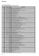
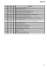
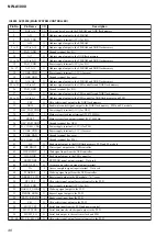
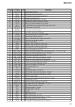
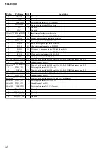
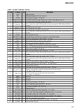
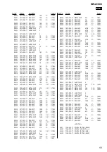
IC6005 SCF5250 (MAIN SYSTEM CONTROLLER)
Pin No.
Pin Name
I/O
Description
1
DATA16
I/O
Two-way data bus with the SD-RAM and NOR flash memory
2
A23
O
Address signal output to the SD-RAM
3
PAD_VDD
-
Power supply terminal (+3V) (for I/O)
4
A22
O
Address signal output to the SD-RAM
5 to 8
A21 to A18
O
Address signal output to the SD-RAM and NOR flash memory
9
PAD_GND
-
Ground terminal (for I/O)
10
A17
O
Address signal output to the NOR flash memory
11 to 14
A16 to A13
O
Address signal output to the SD-RAM and NOR flash memory
15
PAD_VDD
-
Power supply terminal (+3V) (for I/O)
16, 17
A12, A11
O
Address signal output to the SD-RAM and NOR flash memory
18
CORE_VDD
-
Power supply terminal (+1.1V) (for core)
19
CORE_GND
-
Ground terminal (for core)
20, 21
A10, A9
O
Address signal output to the SD-RAM and NOR flash memory
22 to 25
A8 to A5
O
Address signal output to the USB controller and NOR flash memory
26
PAD_GND
-
Ground terminal (for I/O)
27
A4
O
Address signal output to the USB controller and NOR flash memory
28 to 30
A3 to A1
O
Address signal output to the USB controller, NOR flash memory and PLD
31
CS0
O
Chip select signal output to the NOR flash memory
32
XRW
O
Read/write control signal output to the NOR flash memory, PLD and EL module
33
OSC_PAD_VDD
-
Power supply terminal (+3V) (for OSC)
34
CRIN
I
Main system clock input terminal (22.5792 MHz)
35
CROUT
O
Main system clock output terminal (22.5792 MHz)
36
OSC_PAD_GND
-
Ground terminal (for OSC)
37
PLL_CORE1_VDD
-
Power supply terminal (+1.1V) (for PLL)
38
CORE_VDD
-
Power supply terminal (+1.1V) (for core)
39
CORE_GND
-
Ground terminal (for core)
40
PLL_CORE1_GND
-
Ground terminal (for PLL)
41
OE
O
Read signal output to the NOR flash memory, PLD and EL module
42
IDE_DIOW
O
Write signal output to the USB controller
43
IDE_IOPDY
I
Wait signal input from the USB controller
44
IDE_DIOR
O
Read signal output to the USB controller
45
BUFFENB2
O
BUFFENB signal output terminal Not used
46
GSEN_SEL1
O
G-sensor axis selection signal output terminal
47
TA
I
Access complete signal input terminal Not used
48
WAKEUP
I
Wake-up signal input from the USB controller
49
XRESET_LCD
O
Reset signal output to the EL module "L": reset
50
SPI_CS2
O
Chip select signal output for serial control to the PLD
51
PAD_VDD
-
Power supply terminal (+3V) (for I/O)
52
WAKEUP_DENDE
O
Wake-up signal output to the PLD
53
DENDE_SREQ
O
Request signal output to the PLD
54
DATA_READY
I
Ready signal input from the PLD
55
CS1
O
Chip select signal output to the PLD
56
MULTI_SI
I
Serial data input from the PLD and power control
57
MULTI_SCK
O
Serial data transfer clock signal output to the PLD
58
MULTI_SO
O
Serial data output to the real time clock and PLD
59, 60
SPI_CS1, SPI_CS0
O
Chip select signal output for serial control to the PLD

