42
NW-A1000
Pin No.
Pin Name
I/O
Description
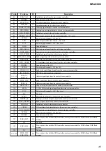
109
LINOUT
O
Not used
110
LININ
I
Not used
111
CORE_VDD
-
Power supply terminal (+1.1V) (for core)
112
SDATAO2
O
Audio data output to the D/A converter
113
NC
I
Not used
114
Hi-Z
-
Not used
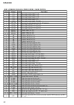
115 to 117 TEST0 to TEST2
I
Input terminal for the test mode setting
118
SDW
O
Write enable signal output to the SD-RAM
119
SDCAS
O
Column address signal output to the SD-RAM
120
PAD_VDD
-
Power supply terminal (+3V) (for I/O)
121
SDRAS
O
Row address signal output to the SD-RAM
122
SDCS0
O
Chip select signal output to the SD-RAM
123
SDLDQ
O
Write mask signal output to the SD-RAM (lower byte)
124
SDUDQ
O
Write mask signal output to the SD-RAM (upper byte)
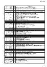
125
BCLKE
O
Clock enable signal output to the SD-RAM
126
BCLK
O
Clock signal output to the SD-RAM
127, 128
DATA31, DATA30
I/O
Two-way data bus with the USB controller, SD-RAM, NOR flash memory and PLD
129
PAD_GND
-
Ground terminal (for I/O)
130 to 134
DATA29 to DATA25
I/O
Two-way data bus with the USB controller, SD-RAM, NOR flash memory and PLD
135
PAD_VDD
-
Power supply terminal (+3V) (for I/O)
136
DATA24
I/O
Two-way data bus with the USB controller, SD-RAM, NOR flash memory and PLD
137 to 140
DATA23 to DATA20
I/O
Two-way data bus with the SD-RAM and NOR flash memory
141
PAD_GND
-
Ground terminal (for I/O)
142 to 144
DATA19 to DATA17
I/O
Two-way data bus with the SD-RAM and NOR flash memory
145 to 163
PAD_VDD
-
Power supply terminal (+3V) (for I/O)
164 to 189
PAD_GND
-
Ground terminal (for I/O)
190 to 192
CORE_VDD
-
Power supply terminal (+1.1V) (for core)
193
BGA_NC_A1
-
Not used
194
BGA_NC_A14
-
Not used
195
BGA_NC_P1
-
Not used
196
BGA_NC_P14
-
Not used

