39
NW-A1000
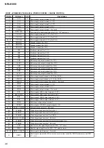
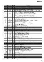
Pin No.
Pin Name
I/O
Description
74
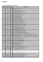
HIORDY
I
Wait signal input from the hard disk drive unit
75
VSS
-
Ground terminal (logic system)
76
VDD
-
Power supply terminal (+3.3V) (logic system)
77
XHDMACK
O
DMA acknowledge signal output to the hard disk drive unit
78
HINTRQ
I
Interrupt request signal input from the hard disk drive unit
79
HA1
O
Address signal output to the hard disk drive unit
80
XHPDIAG
I
Diagnosis sequence compression signal input from the hard disk drive unit
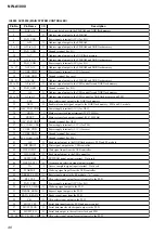
81, 82
HA0, HA2
O
Address signal output to the hard disk drive unit
83, 84
HCS0, HCS1
O
Chip select signal output to the hard disk drive unit
85
XHDASP
I
Drive valid signal and slave drive detection signal input from the hard disk drive unit
86
VSS
-
Ground terminal (logic system)
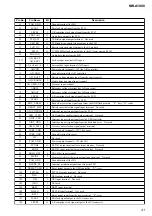
87, 88
CLKSEL0,
CLKSEL1
I
Input terminal for oscillation frequency setting Fixed at 12 MHz in this set
89
VSS
-
Ground terminal (logic system)
90
XVSS
-
Ground terminal (logic system)
91
XVDD
-
Power supply terminal (+3.3V) (logic system)
92
VDD
-
Power supply terminal (+3.3V) (logic system)
93
PVDD
-
Power supply terminal (+3.3V) (for PLL)
94
VDD
-
Power supply terminal (+3.3V) (logic system)
95
PVSS
-
Ground terminal (for PLL)
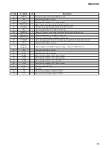
96 to 98
NC
-
Not used
99
XI
I
Sub system clock input terminal (12 MHz)
100
XO
O
Sub system clock output terminal (12 MHz)

