36
NW-A1000
•
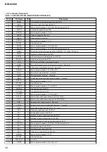
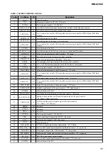
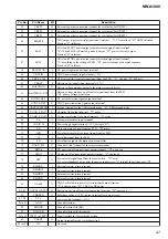
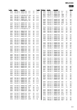
IC Pin Function Description
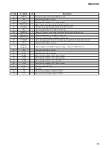
IC3101 CXR710160-215GH (SUB SYSTEM CONTROLLER)
Pin No.
Pin Name
I/O
Description
1
LRCK
I
L/R sampling clock signal input from the PLD
2
BCK
I
Bit clock signal input from the PLD
3
VDIOCD0
-
Power supply terminal (+1.8V) (for CD interface and I/O)
4
PCMD
I
Audio data input from the PLD
5
DVDD4
-
Power supply terminal (+1.3V)
6
TEST8
O
Output terminal for the test
7
TEST7
I
Input terminal for the test
8
DVDD0
-
Power supply terminal (+1.3V)
9
DVSS0
-
Ground terminal
10
VDIO0
-
Power supply terminal (+1.8V) (for I/O)
11
VDIOCD1
-
Power supply terminal (+1.8V) (for CD interface and I/O)
12
XRDE
I
Ready/busy selection signal input from the PLD "L": ready, "H": busy
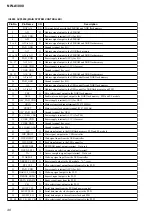
13
BCK0
O
Bit clock signal output to the PLD
14
LRCK0
O
L/R sampling clock signal output to the PLD
15
PCMD0
O
Audio data output to the PLD
16
EVA
I
EVA mode selection signal input terminal
17
KCLK
O
Serial data transfer clock signal output terminal Not used
18
KCS
O
Chip select signal output terminal Not used
19
VDIO01
-
Power supply terminal (+1.8V) (for I/O)
20
KDO
O
Serial data output terminal Not used
21
KDI
I
Serial data input terminal Not used
22
KRB
O
Ready/busy selection signal output terminal Not used
23
DVDD1
-
Power supply terminal (+1.3V)
24
DVSS3
-
Ground terminal
25
AVDPLL
-
Power supply terminal (+3V) (for PLL)
26
AVSPLL
-
Ground terminal (for PLL)
27
AVSOSC
-
Ground terminal (for OSC)
28
AVDMO
-
Power supply terminal (+3V) (for OSC)
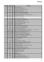
29
EXTAL
I
Main system clock input terminal (22.5792 MHz)
30
XTAL
O
Main system clock output terminal (22.5792 MHz)
31
XIN
I
External clock input terminal Not used
32
OSSEL
I
External clock control signal input terminal Not used
33
NRST
I
Reset signal input from the PLD "L": reset
34
PF0
I
Wake-up signal input from the PLD
35
PF1
O
Ready signal output to the PLD
36
PF2
I
Interrupt request signal input from the PLD
37
PF3
O
Interrupt request signal output to the PLD
38
PC0
I
Serial data transfer clock signal input from the PLD
39
VDIOCD2
-
Power supply terminal (+1.8V) (for CD interface and I/O)
40
PC1
O
Serial data output to the PLD
41
PC2
I
Serial data input from the PLD
42
PC3
O
Chip select signal output to the PLD
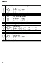
43
DVDD2
-
Power supply terminal (+1.3V)
44
DVSS2
-
Ground terminal
45 to 48
PE0 to PE3
I/O
Not used
49
VDIO2
-
Power supply terminal (+1.8V) (for I/O)

