Sharp ER-A450 Service Manual Download Page 43

8

7

6

5

4

3

2

1

A

B

C

D

1

2

3

4

5

6

7

8

D

C

B

A

/JPES

/RPES

+5V

+5V

Vrf

+24V

B14

B15

C227

47P

6-3B

6-3C

2-3C

C237
330P

R305
4.7K

R306
4.7K

C205
330P

  1

  2

3

1
4

IC28A

74HC00S

C236

10u16V

(C231)

10u16V

5

6

  7

4

8

IC20B
GL393

R339
100K

R340
100K

C267

0.1uF

C268
0.1uF

3

2

  1

4

8

IC20A

GL393

BA14
BA12
BA7
BA6
BA5
BA4
BA3
BA2
BA1
BA0

BD0
BD1
BD2

BD5

BD6

BD7

BA8
BA9
BA11

BA10

10KX9

VDD

A14

  1

A12

  2

A7

  3

A6

  4

A5

  5

A4

  6

A3

  7

A2

  8

A1

  9

A0

 10

D0

 11

D1

 12

D2

 13

GND

 14

VCC

28

/WE

27

A13

26

A8

25

A9

24

A11

23

OE

22

A10

21

CS

20

D7

19

D6

18

D5

17

D4

16

D3

15

IC21

RAM(256K)

SOP

R309

R310

R311

R312

R313

R314

R316

R317

/RESET

JP3
JP4

5-6A

BA13

BD0
BD1
BD2

BD3
BD4

BD5
BD6
BD7

R307

0 OHM

R308

1K

5V

(R315)

GATE ARRAY(TPRC1)

+5V

+5V

+5V

R253

10K

C245
330P

GND

  1

GND

  2

ST1

  3

GND

  4

ST2

  5

ST3

  6

ST4

  7

ST5

  8

ST6

  9

LATCH

 10

GND

 11

GND

 12

GND

 13

SI

 14

SO

 15

CLOCK

 16

INHDEC

 17

CSEN

 18

TEST2

 19

VCC

 20

VCC

 21

VCC

 22

VCC

 23

TEST1

 24

D0

 25

D1

 26

D2

 27

D3

 28

D4

 29

GND

 31

GND

 32

D5

 33

D6

 34

D7

 35

A0

 36

A1

 37

A2

 38

NU

 39

INT1

 40

WI

 41

BACK

 42

A3

 43

A4

 44

A5

 45

A6

 46

A8

 48

A7

 47

A9

 49

GND

 50

GND

 51

GND

 52

A10

 53

A11

 54

A12

 55

A13

 56

A14

 57

A15

 58

A16

 59

VCC

 60

PTJM

120

PTRM

119

BA13

118

BA14

117

BA15

116

BRD

115

BWR

114

CGS

113

GND

112

GND

111

GND

110

JAS

109

JBS

108

JCS

107

JDS

106

RAS

105

RBS

104

VCC

103

VCC

102

VCC

101

VCC

100

VCC

99

GND

98

RCS

97

RDS

96

CTAO

95

CTBO

94

RPE

83

EBACK

82

EBREQ

81

NU

 80

BREQ

 79

INH

 78

WO

 77

INT

 76

POF

 75

AS

 74

WR

 73

RD

 72

GND

 71

GND

 70

A23

 69

A22

 68

A21

 67

A20

 66

A19

 65

A18

 64

A17

 63

VCC

 62

VCC

 61

JPE

84

VHCOM

93

JVPON

92

GND

91

GND

90

GND

89

RVPON

88

PFP

87

PCRES

86

PHUP

85

GND

 30

NU

160

GND

159

RESET

158

BRAS

157

BRAS

156

BD0

155

BD1

154

BD2

153

GND

152

GND

151

GND

150

BD3

149

BD4

148

GND

147

BD5

146

BD6

145

BD7

144

BA0

143

VCC

142

VCC

141

VCC

140

PHAI

139

BA1

138

BA2

137

BA3

136

BA4

135

BA5

134

BA6

133

GND

132

GND

131

GND

130

BA7

129

BA8

128

BA9

127

BA10

126

BA11

125

BA12

124

POPI

123

GND

122

GND

121

IC17

G.A(TPRC1)

C230
0.1u

C264
C265

/STRB1

/STRB2
/STRB3
/STRB4

/LATCH

CLOCK

SO

+5V

+5V

+5V

+5V

+5V

+5V

SI

+5V

6-3B

B19

B20

B23

R246

10K

R247

10K

R248
10K

R249

10K

R250
10K

R251
10K

R252
10K

C238
330P

C239
330P

C240
330P

C241
330P

C242
330P

C243
330P

C244
330P

B24
B25
B26

B21
B22

/BACK

A1

A2

A3

A4

A5

A6

A7

A8

A18

A19

A9
A10
A11
A12
A13
A14
A15
A16
A17

A0

D0

D7

D0
D1
D2
D3
D4

D5
D6
D7

A0
A1
A2

A3
A4
A5
A6
A7
A8
A9

A[0..23]

D[0..7]

2-6B

+5V

NC

  1

A18

  2

A17

  3

A7

  4

A6

  5

A5

  6

A4

  7

A3

  8

A2

  9

A1

 10

A0

 11

CE/CE

 12

OE/OE

 14

D0

 15

D8

 16

D9

 18

NC

44

A19

43

A8

42

A9

41

A10

40

A11

39

A12

38

A13

37

A15

35

A16

34

BHE

33

D15/A-1

31

D7

30

D14

29

D6

28

D13

27

VSS

 13

D1

 17

D2

 19

D10

 20

D3

 21

VCC

23

D4

24

D12

25

D5

26

VSS

32

A14

36

D11

 22

IC25

ROM16M

PHAI

BD3

BD4

VRESC

+5V

BA1
BA2
BA3
BA4
BA5
BA6

BA7
BA8
BA9
BA10
BA11
BA12

BA13
BA14

/BRD
/BWR
CGS

B8
B9
B10
B11

C208
C209
C210

C211

C212

C213

JAS
JBS
JDS
JCS

47pX9

COM

COM

C217
C218

C219

2-1C

  2
  4
  6
  8

1

10

 3
 5
 7
 9

IC22

4AC16

Q31
A1036
SMD

R297

R298
R299

R300
5.6K

R303

1K

PTJM

R320

1KX4

PTRM

+5V

/JPFA
/JPFB
/JPFD
/JPFC

+5V

+24V

PTJM

C228

1000P

6-3C

3-7C

7-4C

R301
100K

R302

33K

R318
5.6K

D9

R304

240

  1

  3

2

IC26

KIA431A

  3

  2

1

4

8

IC19A
GL393

VHC

+24V

+24V

VJCOM

/RPFA
/RPFB
/RPFC
/RPFD

+24V

  5

  6

7

4

8

IC19B
GL393

6-3C

7-7A

6-3B

R286
5.6K

R295

33K

+5V

PTRM

R319
5.6K

7-4C

R287

10K

B2

Q29
C2412K

Q30

2SJ328-Z

C235
2200u/50V

R294

100K

D10
1SS
353

R285

10K

PHUPS

JAS
JBS
JDS
JCS

CUTS

RAS
RBS

RCS
RDS

+5V

+5V

+5V

+5V

B4
B5
B6
B7

RAS
RBS
RCS
RDS

COM

B16

B17

6-3C

6-3B

  2
  4
  6
  8

1

10

 3
 5
 7
 9

IC23

4AC16

R288
10K

R291

1K

R292
1K

R293
1K

R296

R321
R322
R323

1KX4

R284
2.2K

R289 1K

R290

1K

/BREQ

/RD
/WR
/AS

/TPRCRQ

+5V

/TWAIT

+5V

+5V

TM1

+24V

D1

D2

D3

D4

D5

D6

A10
A11
A12
A13
A14
A15
A16

A17
A18
A19
A20
A21
A22
A23

  5

  6

7

8

4

IC18B
GL393

C216
100P

C229
0.1u

/POFF

2-1D
2-1D
2-1D

1-5A
3-1C

3-3D

2-6A

6-3C

B18

R254
18KF

R255

68F

R256

4.7K

C232
10u10V

TM

VH

  3

  2

1

8

4

IC18A

GL393

B1

+5V

C226
0.1u

7-2B

2-3C

6-3C

F2

FUSE

C233

10u100V

R257

1.15KF

R258

133F

R259

4.7K

R260
20K

VHC

NU

  4

  5

6

1
4

IC28B

74HC00S

  9

 10

8

1

4

IC28C

74HC00S

 12

 13

11

1

4

IC28D

74HC00S

7PIN:GND

+5V

BA2
BA3
BA4
BA5
BA6
BA7
BA8
BA9
BA10
BA11
BA12
BA13
BA14

C192
C193
C194
C195
C196
C197
C198
C199
C200
C201
C202

C203

/BRD
/BWR
CGS

+5V

10kX13

47pX13

10kX5

BA0
BA1

C220

C222
C223

C224

C225

R261
R262
R263
R264
R265
R266
R267
R268
R269
R270
R271
R272
R273

R275

C221

47pX5

R278

R276

R277

R274

+24V

CUTM-

CUTM+

C206
0.1u

B3

B12

6-3C

R283
2.2K

C204
47P

C215

47P

C214

47P

AUTO CUT

Q27
C2412K

R279

10K

  3

  5

4

7

1

2
6

(IC24)

TA8248K

C207

0.1u

C234

10u50V

VRCOM

+5V

B13

6-3B

Q28

2SJ263

R282

10K

D11

1SS353

(R280)

1W 8.2

R281

33K

JP5

7/10

6-3B
6-3C
6-3C

6-3B

6-3B

6-3B

6-3C

2-8D

2-8C

6-3C

7-1C

6-3C
6-3C
6-3C

6-3B
6-3B
6-3B

1SS353

Not
mounted

8 – 7

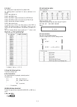
Summary of Contents for ER-A450

Page 1: ...IFICATIONS 1 1 CHAPTER 2 OPTIONS 2 1 CHAPTER 3 SERVICE SRV MODE 3 1 CHAPTER 4 HARDWARE DESCRIPTION 4 1 CHAPTER 5 TEST FUNCTION 5 1 CHAPTER 6 DOWN LOAD FUNCTION 6 1 CHAPTER 7 SERVICE PRECAUTION 7 1 CHAPTER 8 CIRCUIT DIAGRAM PWB LAYOUT 8 1 PARTS GUIDE SHARP CORPORATION CONTENTS This document has been published to be used for after sales service only The contents are subject to change without notice ...

Page 2: ...per feed key RCPT Receipt print and Receipt on off key 1 2 Percent keys Discount key PO Paid out key RF Refund key Non add code entry key NS No sale key RA Recived on account key Void key AUTO1 AUTO2 Automatically entry keys PLU SUB PLU Subdepartment code entry key AMT Amount entry key VAT Value added tax key EX1 EX2 Foreign currency exchange keys CASH Cashier code entry key CR1 CR2 CR3 Credit key...

Page 3: ...haracter size 14 2 H 8 0 W mm Display contents Display Position Description Amount 1 8 Minus sign 4 10 Floating Error 10 E PGM Mode 10 P VOID Mode 10 u TL CH CR 10 F Lights up when a registration is finalized by depressing TL CH CR key SUB TOTAL short tender 10 o Change 10 C Light up whenever the change due amount appears in the display Department 9 10 No zero suppressed PLU 5 10 No zero suppresse...

Page 4: ...nsor Standard equipment 2 Money case Separation from the drawer Allowed Separation of the coin compartments from the money case Allowed Bill separator Number of compartments 5B 8C 3 Lock Location of the lock Front Method of locking and unlocking Locking Insert the drawer lock key into the lock and turn it 90 degrees counterclockwise Unlocking Insert the drawer lock key into the lock and turn it 90...

Page 5: ...nfiguration Fig 1 1 NOTE1 This symbol shows NEW MODEL COMPUTER LOCAL PURCHASE OPTION RAM ER 03RA ER A450 MASTER MACHINE CABLE 3 5 inch FDD ER 01 02FD COMMERCIAL PRODUCT ER 05DW REMOTE DRAWER DKiT 8669BHZZ 1 HOLE CASHIER SWITCH 2 1 ...

Page 6: ...7126BHZZ BE Include the switch cover 4 JOURNAL NEAR END SENSOR UNIT DUNTK3677BH03 BB Q ty 1 Screw Sensor unit Top cabinet XEBSD30P08000 AA Q ty 1 Screw Sensor unit Earth wire Top cabinet XHBSD30P04000 AA Q ty 1 Screw Earth wire Top cabinet LX BZ6778BHZZ AA Q ty 1 Earth wire QCNW 7895BHZZ AF Q ty 1 Connector 2pin QCNCM6865RC0B AA Q ty 1 5 TEXT PRESET KEYBOARD COVER GCOVB7153BHZZ BH 6 ONE HOLE CASHI...

Page 7: ... position MRS 2 Used to clear all memory and keyboard contents This reset returns all programming back to defaults The keyboard must be entered by hand This reset is used if an application needs different keyboard layout other than that supplied by a normal MRS 1 Procedure 1 Unplug the AC cord from the wall outlet 2 Set the MODE switch to the SRV position 3 Plug in the AC cord to the wall outlet 4...

Page 8: ...diagram Fig 1 1 CPU GATE ARRAY MPCA7 DRAWER STANDARD RAM1 128KB OPTIONAL RAM2 512KB ER 03RA 512KB STANDARD ROM 512KB SWITCH KEY BOARD RS232 I F 1 ports CKDC8 1 LINE 7SEG 7DIG 1 LINE 7SEG 10DIG CUSTOMER DISPLAY OPERATER DISPLAY TPRC1 PRINTER PR 45M 4 1 ...

Page 9: ... TXD1 RXD1 SCK2 UASKC IRQ1 IRQ0 VCC AVCC AN3 AN2 112 111 110 109 108 107 106 105 104 103 102 101 100 99 98 97 96 95 94 93 92 91 90 89 88 87 86 85 P41 P42 P43 P44 P45 P46 P47 VSS P50 P51 P52 P53 P54 P55 P56 P57 STOP P60 P61 P62 P63 P64 P65 P66 P67 VSS AVSS AN0 AN1 57 58 59 60 61 62 63 64 65 66 67 68 69 70 71 72 73 74 75 76 77 78 78 80 81 82 83 84 A8 A9 A10 A11 A12 A13 A14 A15 VSS A16 A17 A18 A19 A2...

Page 10: ...17 P16 P15 P14 P13 P12 P11 P10 D7 D6 D5 D4 D3 D2 D1 D0 STOP P57 P56 FMRS P54 P53 P52 P51 P50 P67 P66 RS P65 RR P64 CD P63 CS P62 DR P61 ER P60 P73 AN2 AN1 AN0 TXD2 RXD2 TXD1 RXD1 SCK2 IRQ2 IRQ1 IRQ0 H8 500 CPU DTC Serial communication interface x 2ch 8bit timer 16bit free running timer x 2ch Refresh controller Wait state controller A D convertor Interruption controller Clock oscillator Watch dog t...

Page 11: ... Nu GND 55 VCC VCC 5V 56 P40 IFV IN Nu pull up 57 P41 PTMG IN Printer PR 45 timing signal from MPCA 58 P42 TOF IN Nu pull up 59 P43 BOF IN Nu pull up PIN No SYMBOL SIGNAL NAME IN OUT FUNCTION 60 P44 PRST IN Printer PR 45 Reset signal from MPCA 61 P45 NEJ IN Near END signal jounal 62 P46 NU IN NU GND 63 P47 NER IN Near END signal receipt 64 VSS VSS GND 65 P50 TRG1 OUT Nu GND 66 P51 PSTOP OUT Nu GND...

Page 12: ...TD 136 RJMTS 135 DT5 134 DT6 133 DT7 132 GND 131 DT1 130 DT2 129 DT3 128 DT4 127 RJTMG 126 RJRST 125 RAS1 124 RAS2 123 ROS2 122 ROS1 121 OPTCS 41 D3 42 GND 43 D4 44 D5 45 D6 46 D7 47 SSPRQ 48 RESET 49 INT2 50 INT3 51 RXDI 52 TXDI 53 SCKI 54 IRQ0 55 A0 56 A1 57 A2 58 A3 59 A4 60 A5 61 GND 62 VCC 63 A6 64 A7 65 A8 66 A9 67 A10 68 A11 69 A12 70 A13 71 A14 72 A15 73 A16 74 A17 75 A18 76 A19 77 A20 78 ...

Page 13: ...INT2 EXINT3 SDT1 7 DT1 9 TEST IRQ0 A23 A0 SSPRQ SLF SLRS VF RF JF FCUT PCUT STAMP TRGI TRG TRG DOTEN IRLON D0 D7 Φ Address decode External CS Internal CS RASEL Image control SSP comparison register BAR Buffer Read write control Divider CHS serial select Multiplexer WAIT control CAPS select Print gate Print pulse control Print mode PMD INTO control Printer control port Motor drive Output selection ...

Page 14: ...3 42 GND GND 43 D4 I O Data bus 4 44 D5 I O Data bus 5 45 D6 I O Data bus 6 46 D7 I O Data bus 7 47 SPRQ Out SSP interrupt request to CPU 48 RESET In MPCA reset 49 SHEN In Shift enable from CKDC8 50 INT3 In Interrupt signal Nu Pin No Signal name In Out Function 51 RXD2 Out 8 bit serial port output to CPU 52 TXD2 In 8 bit serial port input from CPU 53 SCK2 In Serial port shift clock input from CPU ...

Page 15: ...Serial output to FMC unit 151 SCK2 Out Serial clock to FMC unit 152 STH2 In Serial input to FMC unit 153 Nu 154 Nu 155 Nu 156 Nu 157 Nu 158 LCDWT IN TPRC wait signal 159 DOTEN Out Dot drive enable signal Nu 160 RASP Nu 2 3 CKDC8 1 Pin configulation 2 Pin assignment CKDC8 Pin No SYMBOL SIGNAL NAME IN OUT FUNCTION 1 DP DP OUT DISPLAY SEGMENT Dp 2 A SA OUT DISPLAY SEGMENT a 3 B SB OUT DISPLAY SEGMENT...

Page 16: ...IGIT 7 60 T7 G8 OUT DISPLAY DIGIT 8 61 T8 G9 OUT DISPLAY DIGIT 9 62 T9 G10 OUT DISPLAY DIGIT 10 63 T10 NU OUT DISPLAY DIGIT 11 64 ID NU OUT DISPLAY SEGMENT c 2 4 TPRC1 F258024PC 1 General TPRC1 is the LSI circuit of the peripheral circuits of the microcomputer required for thermal printer control Fig 2 6 The CPU is designed for use with H8 500 The bus I F however is not restricted to the design co...

Page 17: ...P P 122 121 41 42 BACK 43 A3 44 A4 45 A5 46 A6 47 A7 48 A8 49 A9 50 51 52 53 A10 54 A11 55 A12 56 A13 57 A14 58 A15 59 A16 60 61 62 63 A17 64 A18 65 A19 66 A20 67 A21 68 A22 69 A23 70 71 72 RD 73 WR 74 AS 75 POF 76 INT 77 WO 78 79 BREQ 80 120 PTJM 119 PTRM 118 BA13 117 BA14 116 BA15 115 BRD 114 BWR 113 CGS 112 111 110 109 JAS 108 JBS 107 JCS 106 JDS 105 RAS 104 RBS 103 102 101 100 99 98 97 RCS 96 ...

Page 18: ...ve strobe signal 4 8 ST5 O NU 9 ST6 O NU 10 LATCH O Head latch signal 11 GND GND 12 GND GND 13 GND GND 14 SI I Data return line thermalhead TPRC1 15 SO O Send data from TPRC1 to thermalhead Data from PB RAM or zero data are outputted at the falling of CLOCK signal 16 16 CLOCK O Thermalhead CLOCK signal SO is outputted at the edge of I Ä O and is taken at the edge of o Ä I Pin No Signal name In Out...

Page 19: ...option 83 RPE I Receipt paper empty 84 JPE I Journal paper empty 85 PHUP I Printer head up 86 PCRES I Auto cutter unit reset signal input Nu 87 PFP I Auto cutter unit FP signal input Nu 88 RVPON O Receipt side paper feed pulse motor common power control signal Nu 89 GND GND 90 GND GND 91 GND GND 92 JVPON O Journal side paper feed pulse motor common power control signal Nu 93 VHCOM O Head drive com...

Page 20: ...appear on this line in most cases 2 CKDC8 oscillation circuit Fig 3 2 Two oscillators are connected to the CKDC8 The main clock X1 generates 4 19MHz which is used during power on When power is turned off the CKDC8 goes into the standby mode and the main clock stops The sub clock X2 generates 32 768KHz which is primarily used to update the internal RTC real time clock During the standby mode it kee...

Page 21: ...jected to 000000H 007FFFH for allowing reset start and other vector addressing or the lower 32KB of ROM area which is projected to 008000H 00FE7FH for allowing 0 page addressing of work RAM area 4 Expansion I O means expansion I O device area which isad dressed to area other than page 0 2 0 page memory map Fig 5 2 ROM image area Image is formed in ROM area address C00000H to C07FFFH This area is i...

Page 22: ...chip select signals RAS2 and RAS3 The control register in MPCA7 allows selection of pageimage memory area RAS1 is selected for initializing For 0 page image area selection between RAS2 and RAS3 can bemade with the control register The 0 page control registerper forms initializing at the timing of no stack processimmediately after resetting 100000H 400000H BFFFFFH NOT USE NOT USE RAS1 Not use RAS2 ...

Page 23: ...s FFFF00H or later decoded in MPCA7 2 SSP register The break address register BAR is accessed through direct address of FFFF00H FFFFFFH Entry number is 32 entry Fig 6 3 Each BAR is composed of 4 byte address Bit composition is as fol lows Fig 6 4 4 is the enable register The entry registers of the break address are assigned to 1 2 and 3 Each bit of address corresponds to each bit position writing ...

Page 24: ... are 32 break registers binary expression is made with the above 5 bits and 0th is 00000B and 31st is 11111B When detected simultaneously by two or more break registers onewith the smaller BAR number is read as binary data The brake signals NMI and the above detection data CMP0 4 are held until the above detection data are read So read should bemade in the NMI sub routine Clear by FFFFFFH read 1 F...

Page 25: ... turning on the power the CKDC8 cancels resetting of the CPU in the command mode After initializing each port the CPU reads the start condition 1 byte Fig 9 2 After sampling POF High the CKDC8 performs mode scan and key scan at 1 then cancels resetting of the CPU After being cancelled the CPU initializes each port at 2 and reads the start condition After being cancelled the CPU reads the start con...

Page 26: ... the CPU If reset request is not sent from the CPU within 100msec the service interruption procedure is started after 110 10msec to go into the stand by mode Fig 9 4 3 Key and switch scanning Fig 9 5 As the strobe signal 8 bits of ST0 8 are used KR0 KR7 are used as the key return signal KR10 is used as the return signal of the paper feed key cashier key and MRS switch KR11 is used as the return si...

Page 27: ...rn power on in the SRV mode and change it to the SRV mode Journal print PRG RESET 3 Test command list With the SRV mode and the following test code entry the test start CODE DESCRIPTION 100 Display Buzzer test 101 Key code Cashier key test 102 R J printer test 104 Keyboard test 105 Mode switch test 106 Printer sensor test 108 Calendar osckllator test 109 SSP test 110 Drawer open sensor test For st...

Page 28: ...med 4 Keyboard test 1 Key operation XXXX Sumcheck data Standard keyboard layout sumcheck data ER A450 2243 2 Functional description Keyboard test is performed with the sumcheck data of key code For sumcheck data data are inputted to the upper upper four digits befor the diagnostics code The data are compared with the added data which are added until the final key TL is pressed if the data agree wi...

Page 29: ...isplayed Description W NER 0 Receipt paper near end sensor Detected 1 Receipt paper near end sensor Not detected X NEJ 0 Journal paper near end sensor Detected 1 Journal paper near end sensor Not detected Y RPES 0 Receipt paper end sensor Detected 1 Receipt paper end sensor Not detected Z JPES 0 Journal paper end sensor Detected 1 Journal paper end sensor Not detected 1 is always display when no s...

Page 30: ... to terminate the program without check 9 Drawer open sensor test For standard test 1 Key operation 2 Functional description State of the drawer open sensor is sensed and displayed 3 Check items X Description O Drawer open sensor detected Drawer opend C Drawer open sensor not detected Drawer closed a Check opening of the specified drawer b Check the display indication when the drawer is open and c...

Page 31: ...r two digits of SUM is 10H it is normal 3 Check the following items Check the printout after the test 4 Test termination The test automatically terminates with termination message Normal termination print 130 ROM1 27040 Error termination print E 130 ROM1 27040 Note means the ROM version number The underlined section 10 bytes of code table is provided in the ROM as a standard and the table content ...

Page 32: ...800H 201000H 202000H 204000H 208000H 210000H 220000H 240000H 260000H 3 Check the following items Check the termination print 4 Test termination The test terminates after printing the termination printout Termination print E1 200 data check error E2 200 address check error 200 normal end Error address 15 RS 232 loop back test Connect the loop back connector UKOG 6705RCZZ to RS232 con nector 1 Key o...

Page 33: ... Selected by SRV JOB 903 A 4 Sync mode Asynchronous 5 Checking Vertical parity odd 6 Code 7 bits ASCII 7 Bit sequence LSB first 8 Line level RS232 level 9 Data forma FIg 2 1 3 Location of connector pins 1 ECR ECR cable Fig 3 1 ECR ECR ECR ER 02FD P b1 b2 b3 b4 b5 b6 b7 LSB MSB Start bit Parity bit Stop bit SD 3 SD RD CTS RD 2 6 8 3 2 6 8 5 5 SG RTS 7 DCD 1 DTR 4 DSR 7 1 4 ECR CTS SG RTS DCD DTR DS...

Page 34: ...r words 128 bytes are sent at one time on the transmit data format RAM DATA FORMAT Exhibit Code table HEX ASCII Character HEX ASCII Character 0 30 0 8 38 8 1 31 1 9 39 9 2 32 2 A 41 A 3 33 3 B 42 B 4 34 4 C 43 C 5 35 5 D 44 D 6 36 6 E 45 E 7 37 7 F 46 F 6 END record 1 End message Fixed to 30303030 2 End massage Fixed to 4646 3 Sum check 4 End code CR 0D SD 2 SD RD CTS RD 3 6 5 3 2 6 8 ER 02FD 7 5 ...

Page 35: ...and set the DIP switches of the FD unit as follows ER 02FD The ER 01FD functions of the ER 02FD are used 2 Connect the cable Saving data 1 Turn on the power switch and insert a floppy disk which has been formatted 2 Start the SEND JOB on the ECR side as follows X 0 SSP 3 Data transmission is started and the green lamp on the ER 02FD blinks Loading data 1 Turn on the power switch and insert the flo...

Page 36: ...ry E37 The direct finalization is inhibited Make a tendering operation E58 Undefined clerk code is entered Enter a correct clerk code E67 Registration buffer is full E76 The drawer is still opened Close the drawer E86 Communication error SRV 996 998 E87 Data format error SRV 996 998 E88 Time out error SRV 996 998 2 Conditions for soldering circuit parts To solder the following parts manually follo...

Page 37: ...6 5 2 3 4 1 7 8 IC6 KA34063A Q23 C4153 HEAT SINK C266 100uF 50V 1 2 CN8 PS CN 24V F1 FUSE T800mA 250V FROM PS PWB 24V GND C85 220P R113 1KF C84 0 1uF 50V VBT R120 150 C82 330uF 16V C81 330uF 16V C86 0 1uF 50V 2 1 CN9 BTCN 5V P0FF 3 2 1 8 4 IC7A KIA393F 3 8D R118 56K 24V D7 1SS353 R119 2 7K 5 6 7 8 4 IC7B KIA393F 24V P OFF CIRCUIT C83 1u 50V R117 2 7K R114 8 2KG R115 15KG R116 9 1KG ZD1 UDZ5 1B C87...

Page 38: ...0 R172 R171 R195 5V 10K X8 ERC LDRQ 8 4B 8 4B R139 100 R140 100 R141 100 R142 100 R143 100 R144 100 R145 100 R146 100 PDS 8 2B SHEN 8 8B FRES BUSY_A RDY_A R173 R174 R175 R176 R177 R178 R179 R180 Vrf FIL2 100P 1 3 2 X4 19 66MHz TM FVHS 7 1D 7 8A 6 3B R126 4 7K 5V D28 1SS353 R160 3 6K F R159 16K F 24V TXD2 RXD2 IRQ0 IRQ1 PHAI 5V 5V 5V RXD TXD 5V 5V 5V 5V 3 8B 6 2C 3 8B 10 8C 10 8B 3 8B 3 8C SCK2 5V ...

Page 39: ... U 157 N U 156 N U 155 N U 154 N U 153 STH2 152 SCK2 151 HTS2 150 SLMTR 149 SLMTS 148 SLMTD 147 RJMTR 146 RAS3 145 NU 144 VSS 143 VCC 142 ASKRX 141 SYNC 140 DOT8 139 DOT9 138 RJMTD 137 RJMTS 136 DOT5 135 DOT6 134 D0T7 133 VSS 132 DOT1 131 DOT2 130 DOT3 129 DOT4 128 RJTMG 127 RJRST 126 RAS1 125 RAS2 124 ROS2 123 ROS1 122 OPTCS 121 IC10 G A MPCA7 RES 5V 5V 5V 5V 5V 6 2C R208 10K R205 10K R206 10K R2...

Page 40: ...R232 820 C172 10u 50V R234 3 3K C171 0 1u 50V R233 1 2K R241 68 F VCH FRES FSD FRD FSCK BUSY 2 5C 3 1D 3 1D 3 1D 2 5A 3 3A RDY 2 5A R239 56K R240 56K R237 56K R238 56K GND 1 VPP 2 VCH 3 FRES 4 FSD 5 FRD 6 FSCK 7 BUSY 8 RDY 9 VCON 10 VPF 11 CN14 FMC CN 5V JP2 Q25 A1036 Q26 KRC106S R236 10K R235 3 9K 4 10 Not mounted NOT USED ...

Page 41: ... 9 A2 10 A1 11 A0 12 D0 13 D1 14 D2 15 GND 16 VCC 32 A18 PGM 31 A17 30 A14 29 A13 28 A8 27 A9 26 A11 25 OE 24 A10 23 CE 22 D7 21 D6 20 D5 19 D4 18 D3 17 IC13 ROM1 32P DIP C176 47U 16V C177 0 1u ROS1 A0 A1 A2 A3 A4 A5 A6 A7 A12 A15 A16 D0 D1 D2 3 1C 4M A8 A9 A10 A11 A13 A14 A17 A18 D3 D4 D5 D6 D7 A14 A12 A7 A6 A5 A4 A3 A2 A1 A0 D0 D1 D2 5V A16 2M C182 10U 16V C181 0 1uF C178 0 1uF C179 10U 16V D7 D...

Page 42: ...COM CUTS CUTM CUTM STRB3 STRB4 VH TM1 SO SI WR0 RESET RD0 TRQ1 RES IRQ1 POFF EXINT0 OPTCS A0 A1 A2 A3 A4 A5 D7 VH SO SI CUTM CUTM CUTS VJCOM JPFA JPFB JPFD JPFC JPES TM1 STRB4 STRB3 WR0 RESET RD0 TRQ1 IRQ1 RES POFF EXINT0 OPTCS VDD 5V 24V 5V 3 5V 4 VDD 5 WR0 6 RESET 7 RD0 8 TRQ1 9 RES 10 IRQ1 11 POFF 12 EXINT0 13 OPTCS 14 A0 15 A1 16 A2 17 A3 18 A4 19 A5 20 D7 21 D6 22 D5 23 D4 24 D3 25 D2 26 D1 2...

Page 43: ...A2 A3 A4 A5 A6 A7 A8 A18 A19 A9 A10 A11 A12 A13 A14 A15 A16 A17 A0 D0 D7 D0 D1 D2 D3 D4 D5 D6 D7 A0 A1 A2 A3 A4 A5 A6 A7 A8 A9 A 0 23 D 0 7 2 6B 5V NC 1 A18 2 A17 3 A7 4 A6 5 A5 6 A4 7 A3 8 A2 9 A1 10 A0 11 CE CE 12 OE OE 14 D0 15 D8 16 D9 18 NC 44 A19 43 A8 42 A9 41 A10 40 A11 39 A12 38 A13 37 A15 35 A16 34 BHE 33 D15 A 1 31 D7 30 D14 29 D6 28 D13 27 VSS 13 D1 17 D2 19 D10 20 D3 21 VCC 23 D4 24 D...

Page 44: ...7 POFF VDD VDD R1 10K C1 10U 16V BD8 BD9 BD10 9 5B 9 5B 9 5B 9 5B X2 32 768KHZ KR1 KR2 KR3 C11 22p 2 3 1 X1 4 19MHz R5 1M BD4 BD5 BD6 BD7 D2 1SS353 PDS PDS DP G F E D C B A G6 G5 G4 G3 G2 G1 5V DP 1 G 2 F 3 E 4 D 5 C 6 B 7 A 8 G7 9 G6 10 G5 11 G4 12 G3 13 G2 14 G1 15 CN3 POP CN 15P R3 2 2K FISCAL PDS R4 12K Q10 C2412K TO POP UP LED PWB 1 2 BZ1 BUZZER G7 PDS TO FRONT LED PWB JP1 0 OHM 0 OHM JP6 1 G...

Page 45: ...ST6A ST7A ST8A D23 SW1 MRS SW KEY74 51 50 36 23 9 22 8 37 35 33 NC 15 25 24 61 62 58 60 67 68 27 42 56 55 54 39 43 45 47 49 48 34 21 20 7 5 4 3 NC 57 63 59 66 13 14 28 41 40 38 29 44 46 32 19 18 6 NC NC 64 65 12 26 52 53 31 30 17 16 NC 10 11 NC K R 2 K R 3 K R 4 K R 5 K R 6 K R 7 K R 1 0 K R 0 K R 1 R333 R329 R331 1 1 2 2 3 3 4 4 5 5 6 6 7 7 8 8 9 9 CN20 KEY_CN_9P R325 R327 R330 R332 R328 R326 47K...

Page 46: ... 2 1B 2 1B 2 1B 2 1B C1 12 C1 14 C2 15 C2 16 V 13 V 17 T1IN 7 T2IN 6 T3IN 20 T4IN 21 R1OUT 8 R2OUT 5 R3OUT 26 R4OUT 22 R5OUT 19 EN 24 T1OUT 2 T2OUT 3 T3OUT 1 T4OUT 28 R1IN 9 R2IN 4 R3IN 27 R4IN 23 R5IN 18 SHDN 25 V C C 1 1 1 0 1 0 IC27 MAX211 C252 0 1U C253 0 1U C255 0 1U C254 0 1U R334 R335 R336 R337 R338 100X5 CI FB1 FB2 FB3 FB4 FB5 FB6 FB7 FB8 RS ER SD RD CD CI DR CS C247 C248 C249 C250 1000PX5...

Page 47: ...2 3 G3 4 G4 5 G5 6 G6 7 G7 8 G8 9 G9 10 G10 11 A 12 B 13 C 14 D 15 E 16 F 17 G 18 DP CN1 FRONT CN 18P FND1 G1 G10 G1 G2 FND3 FND2 G3 G4 G5 G6 G7 FRONT PWB FRONT LED PWB FND5 FND4 G8 G9 G10 G DP R7 30 R8 30 C D E F R3 30 R4 30 R5 30 R6 30 A B R1 30 R2 30 A DP 1 1 ...

Page 48: ... 8 7 6 5 4 3 2 1 A B C D 1 2 3 4 5 6 7 8 D C B A POP UP PWB 1 1 DIG7 DIG5 DIG6 DIG2 DIG3 DIG4 DIG1 CN1 POP UP CN FND1 FND3 FND2 FND4 DP R10 27 F G R12 27 R14 27 D E R16 27 R18 27 B C R20 27 R22 27 R24 27 A ...

Page 49: ...80uH PS PWB 2 1 CN17 CAR BT CN POWER UNIT CORE 1 2 CN1 PS CN 4 1 2 3 BD1 CP301 C6 3300UF 50V C2 4700UF 50V C5 3300UF 50V C1 M0 033u F1 SEMKO T2 5AL 250V 6 8PIN NC D1 PS156R 1 5 7 3 4 2 IC1 LM2574HVN R2 10 C3 22UF 50v R1 18K 24V GND 2 1 TO MAIN PWB R4 1 2KF R3 22KF C4 2200uF 50V 1 1 ...

Page 50: ...40 003 800 ELCO VHIN B 3 TM B 4 VDD 5V B 5 STB4 B 6 STB3 B 7 Din B 8 VH B 9 VH A 1 VH A 2 VH A 3 Dout A 4 CLK A 5 LAT A 6 STB2 A 7 STB1 1 2 3 4 5 6 7 8 9 CON2 53047 0910 MOLEX 1 2 3 4 5 6 7 8 9 CON3 53047 0910 MOLEX R5 47K C1 10uF 50V JPFD JPFC JPFB JPFA VJCOM VJCOM 1 2 3 4 5 6 CON6 53014 0610 MOLEX VRCOM VRCOM RPFA RPFB RPFC RPFD 1 2 3 4 5 6 CON7 53014 0610 MOLEX VDD 5V 1 3 4 2 R4 220 R3 39K RPES...

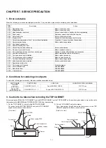
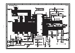
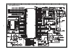
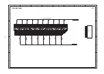
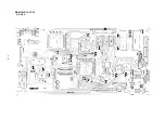
Page 51: ...MAIN PWB LAYOUT 1 SIDE A 8 15 ...

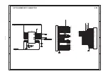
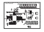
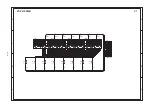
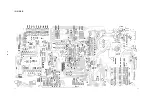
Page 52: ... 2 SIDE B 8 16 ...

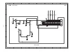
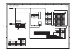
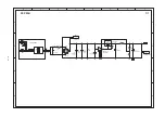
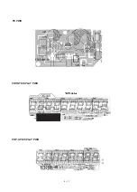
Page 53: ...PS PWB FRONT DISPLAY PWB POP UP DISPLAY PWB 8 17 ...

Page 54: ...R SEEG territory other than Germany Stamp English KB U Kingdom KA Australia SELECTION CODE COUNTRIES K Korea SELECTION CODE COUNTRIES SB Saudi Arabia 127V area SBA Saudi Arabia 220V area SC Taiwan SD Venezuela SE Hong Kong SG Lebanon Syria Greece Pakistan Iran Egypt Thailand Iraq Mauritius Seychelles Tahiti Jordan Sudan Turkey SH South Africa U S A version SHE South Africa Europe version SJ Philip...

Page 55: ...C Screw 4 6 29 R T R N P 9 5 2 4 B H Z Z BK B Power transformer 220V 230V TQ TR TS R T R N P 6 8 9 8 B H Z Z BK N B Power transformer 230V 240V KA KB 30 Q C N W 7 8 7 2 B H Z Z AK C PS cable 31 L B N D J 2 0 0 3 S C Z Z AA C Cable band 32 X N E S D 3 0 2 4 0 0 0 AA C Nut M3 33 L X B Z 6 7 7 8 B H Z Z AA C Screw 3 6 34 X H B S D 3 0 P 0 4 0 0 0 AA C Screw 3 4 35 Q T A N Z 6 6 6 1 B H Z Z AE C Fasto...

Page 56: ...RCPS0234 1 2 5 6 7 8 9 10 13 14 16 17 18 19 20 18 18 18 18 18 18 22 21 18 29 33 23 28 32 34 35 34 35 33 37 36 33 41 27 31 18 30 18 38 18 62 63 64 69 39 71 18 40 47 43 46 47 44 44 45 49 48 41 41 34 34 70 ER A450V 2 ...

Page 57: ...19 L H L D Z 6 8 3 6 B H Z Z AE C Holder R 20 L H L D Z 6 8 3 7 B H Z Z AE C Holder L 101 T L A B H 7 0 9 2 B H Z Z AP N D Key label 501 D U N T K 0 2 4 7 B H Z Z BP N E Key board except No 1 3 5 6 3 Packing material Accessories NO PARTS CODE PRICE RANK NEW MARK PART RANK DESCRIPTION 1 S P A K A 8 4 2 2 B H Z Z AX D Packing add L for SK420 2 P S H E P 6 6 8 1 B H Z Z AF D Packing sheet 3 S P A K A...

Page 58: ...2 Keyboard unit 3 Packing material Accessories RCPS0235 9 5 10 18 3 11 17 15 2 1 20 19 6 7 8 14 16 5 18 18 18 18 18 RCPS0236 1 2 3 4 5 13 18 10 14 12 15 11 6 7 8 9 16 ER A450V 4 ...

Page 59: ... type RCPS0237 1 2 3 4 5 6 7 8 9 11 42 12 13 14 15 16 17 18 19 20 21 22 23 24 25 26 27 28 29 30 31 32 33 34 34 36 37 38 41 3 13 501 12 28 16 10 32 35 33 35 34 35 33 39 39 32 40 32 34 35 40 502 43 44 46 26 33 33 503 ER A450V 5 ...

Page 60: ... 5 1 B H Z Z AF C Earth spring 39 N R O L P 6 6 5 0 B H Z Z AP C Roller 40 X N E S D 6 0 5 0 0 0 0 AA C Nut M6 41 S P A K A 8 3 7 5 B H Z Z AD D Paper pad 42 G C A S P 6 7 0 0 B H Z Z BB D Money case 5B 8C 43 L P L T P 6 7 1 1 B H Z Z AP C Bill guide 44 L A N G K 7 6 1 2 B H Z Z AF C Fixing angle A 46 X H P S D 3 0 P 0 8 0 0 0 AA C Screw 3 8 501 C C A S P 6 7 0 0 B H Z Z BH E Money case unit 5B 8C...

Page 61: ... A D 1 0 1 J AA C Resistor 1 10W 100Ω 5 R131 133 135 139 140 141 142 143 144 145 V R S T S 2 A D 1 0 1 J AA C Resistor 1 10W 100Ω 5 R146 181 182 183 226 227 228 334 335 336 V R S T S 2 A D 1 0 1 J AA C Resistor 1 10W 100Ω 5 R337 338 41 V R S T S 2 A D 1 0 2 F AA C Resistor 1 10W 1KΩ 1 R113 42 V R S T S 2 A D 1 0 2 J AA C Resistor 1 10W 1 0KΩ 5 R127 128 289 290 291 292 293 296 297 298 V R S T S 2 A...

Page 62: ...68KHz X2 102 R C R S Z 6 6 4 4 R C Z Z AD B Crystal 4 19MHz X1 103 R V R M 5 3 1 8 Q C Z Z AC B Variable resistor 5K 8V3P VR1 104 V C E A G A 1 H W 2 2 8 M AB C Capacitor 50WV 2200µF C235 105 V C E A G U 1 C W 1 0 8 M AD C Capacitor 16WV 1000µF C80 106 V H I 2 7 0 4 0 R B K 1 A BM N B IC EP ROM 4M TI27C040 10 IC13 107 V H I 4 A C 1 6 1 AK B IC 4AC16 IC22 23 108 V H I K A 3 4 0 6 3 A 1 AP B IC KA34...

Page 63: ...er 3 G C O V H 7 1 2 6 B H Z Z BE S Drip proof keyboard cover include the switch cover 4 D U N T K 3 6 7 7 B H 0 3 BB S Journal near end sensor unit Q ty 1 X E B S D 3 0 P 0 8 0 0 0 AA C Screw 3 8 Sensor unit Top cabinet Q ty 1 X H B S D 3 0 P 0 4 0 0 0 AA C Screw 3 4 Sensor unit Earth wire Top cabinet Q ty 1 L X B Z 6 7 7 8 B H Z Z AA C Screw Earth wire Top cabinet Q ty 1 Q C N W 7 8 9 5 B H Z Z ...

Page 64: ...ey 14 2pcs 1set with key ring 115 L K G I M 1 0 0 4 B H 1 5 BH S Clerk key 15 2pcs 1set with key ring 116 G F T A F 6 9 2 2 B H S C AH S Clerk cover B 201 L A N G T 2 7 7 9 B H Z Z AP N C Fet angle 202 X E B S D 3 0 P 0 8 0 0 0 AA C Screw M3 8 203 Q C N W 7 9 2 5 B H Z Z BF N C Connector with wire 34pin 204 Q C N C W 7 2 4 3 B H 3 D AV C Connector 34pin 205 Q C N W 7 9 2 6 B H Z Z AF N C GND wire ...

Page 65: ...02 AW S LKGIM1004BH03 11 103 AW S LKGIM1004BH04 11 104 AW S LKGIM1004BH05 11 105 AW S PARTS CODE NO PRICE RANK NEW MARK PART RANK LKGIM1004BH06 11 106 AW S LKGIM1004BH07 11 107 BH S LKGIM1004BH08 11 108 BH S LKGIM1004BH09 11 109 BH S LKGIM1004BH10 11 110 BH S LKGIM1004BH11 11 111 BH S LKGIM1004BH12 11 112 BH S LKGIM1004BH13 11 113 BH S LKGIM1004BH14 11 114 BH S LKGIM1004BH15 11 115 BH S LKGIM7110B...

Page 66: ...AGA1CW106M 5 14 AA C VCEAGA1CW337M 5 15 AB C VCEAGA1CW476M 5 16 AB C PARTS CODE NO PRICE RANK NEW MARK PART RANK VCEAGA1HW105M 5 17 AB C VCEAGA1HW106M 5 18 AA C VCEAGA1HW107M 5 19 AA C VCEAGA1HW226M 7 8 AB C VCEAGA1HW228M 5 104 AB C 7 18 AB C VCEAGU1CW108M 5 105 AD C VCEAGU1HW338M 7 19 AT C VCEAGU2AW106M 5 20 AB C VCKYTV1HB102K 5 28 AA C VCKYTV1HB103K 5 29 AB C VCKYTV1HB222K 5 30 AA C VCKYTV1HF104...

Page 67: ...AA C 11 4 AA C 11 202 AA C XEBSD30P10000 1 41 AA C XHBSD30P04000 1 34 AA C 11 4 AA C XHBSD40P06000 1 28 AA C XHBSD40P08000 4 35 AA C XHPSC30P08000 4 37 AA C XHPSD30P08000 4 46 AA C XHSSD30P06000 4 16 AA C XJPSD30P06000 2 18 AA C XJPSD30P08000 2 5 AA C XJPSD30P12X00 1 47 AB C XNESD30 24000 1 32 AA C XNESD60 50000 4 12 AA C 4 40 AA C XRESJ40 06000 4 11 AA C XRESJ50 06000 4 17 AA C XUBSD30P08000 4 3 ...

Page 68: ... stored in a retrieval system or transmitted in any form or by any means electronic mechanical photocopying recording or otherwise without prior written permission of the publisher SHARP CORPORATION Information Systems Group Quality Reliability Control Center Yamatokoriyama Nara 639 1103 Japan 1998 July Printed in Japan S ...

Reviews: