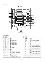
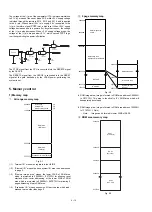
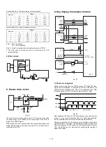


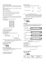
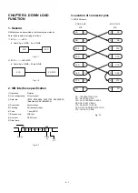
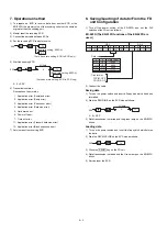


2) Functional description
Perform the following check for the standard RAM 128 KByte SRAM.
The memory contents should not be changed before and after the
check.
Perform the following processes for memory address to be checked
(1E0000H~1F0000H).
PASS1: Save memory data.
PASS2: Write data "0000H."
PASS3: Read and compare data "0000H," write data "5555H."
PASS4: Read and compare data "5555H," write data "AAAAH."
PASS5: Read and compare data "AAAAH."
PASS6: Restore the memory data.
If a compare error occurs in the check sequence PASS1-PASS6, an
error print is made. If no error occurs through all address, the check
ends normally.
The following address check is performed further.
Check point address =
1E0000H, 1E0001H
1E0002H, 1E0004H
1E0008H, 1E0010H
1E0020H, 1E0040H
1E0080H, 1E0100H
1E0200H, 1E0400H
1E0800H, 1E1000H
1E2000H, 1E4000H
1E8000H, 1F0000H
3) Check the following items:
Check the termination printout.
4) Test termination
The test terminates after printing the termination printout.
Termination printout:
Normal termination
120
Abnormal termination
Ex – – – – –
120
*****
X = 1: Data check error
2: Address check error
Note: When an error occurs, the error print is performed and the
check is terminated. The error occurrence address is shown in
hexadecimal at positions shown with
*****
.
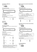
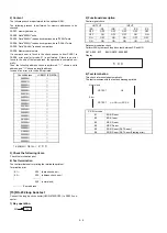
[12] Standard ROM test
1) Key operation
2) Functional description
Sum check of the standard ROM (C00000H - C7FFFFH) is performed.
If the lower two digits of SUM is 10H, it is normal.
3) Check the following items:
Check the printout after the test.
4) Test termination
The test automatically terminates with termination message.
Normal termination print
130
ROM1
27040
*****
*****
Error termination print
E – – – –
130
ROM1
27040
*****
*****
Note: "
*****
" means the ROM version number.
The underlined section (10 bytes) of code table is provided in
the ROM as a standard and the table content is always printed.
The table position is the upper 10 digits of the ROM address.
The check sum correction address is the last address -0FH.
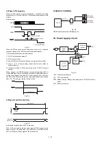
[13] A/D conversion test
1) Key operation
2) Contents
The digital conversion value of the input signal to the CPU A/D conver-
tor is displayed sequentially. The display channel is changes is ap-
prox. 1 sec. interval by timer control and is displayed repeatedly.
Thermistor input
Vrf input: Vrf means the presumed voltage of VRF when VCC is sup-
posed to be +0.5V.
+24V input
Head input
Note: "XXXXX": The 10 bit data of the A/D convertor displayed in
decimal number.
Therefore, its connect may be 0000
~
1024.
3) Confirmation
Check the display content.
4) Termination
To when the mode switch is set to any mode other than SRV mode,
the termination print is made and the test is terminated.
151
Test termination print
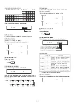
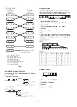
[14] Option RAM test
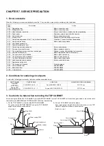
1) Key operation
JOB
#NO.
RAM NO.
Memory to be
checked
Address area to be
checked
200
Option RAM
ER-03RA
200000H
~
27FFFFH
1
0
7-SEGMENT DISPLAY:
2
130
TL
1
0
7-SEGMENT DISPLAY:
3
151
TL
1
1
7-SEGMENT DISPLAY:
5
1
XXXX
1
1
7-SEGMENT DISPLAY:
5
2
XXXX
1
1
7-SEGMENT DISPLAY:
5
3
XXXX
1
1
7-SEGMENT DISPLAY:
5
4
XXXX
200
TL
5 – 5
Summary of Contents for ER-A450
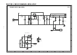
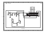
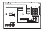
Page 51: ...MAIN PWB LAYOUT 1 SIDE A 8 15 ...
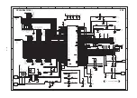
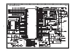
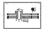
Page 52: ... 2 SIDE B 8 16 ...
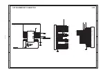
Page 53: ...PS PWB FRONT DISPLAY PWB POP UP DISPLAY PWB 8 17 ...