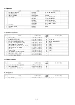

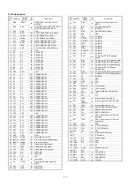
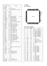


Pin
No.
Signal
name
In/Out
Function
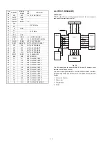
127
BA9
O
Address bus 9 for PB-RAM
128
BA8
O
Address bus 8 for PB-RAM
129
BA7
O
Address bus 7 for PB-RAM
130
GND
—
GND
131
GND
—
GND
132
GND
—
GND
133
BA6
O
Address bus 6 for PB-RAM
134
BA5
O
Address bus 5 for PB-RAM
135
BA4
O
Address bus 4 for PB-RAM
136
BA3
O
Address bus 3 for PB-RAM
137
BA2
O
Address bus 2 for PB-RAM
138
BA1
O
Address bus 1 for PB-RAM
139
PHAI
I
TPRC1 clock input pin (9.83 MHz)
140
Vcc
—
+5V
141
Vcc
—
+5V
142
Vcc
—
+5V
143
BA0
O
Address bus 0 for PB-RAM
144
BD7
I/O
Data bus 7 for PB-RAM
145
BD6
I/O
Data bus 6 for PB-RAM
146
BD5
I/O
Data bus 5 for PB-RAM
147
GND
—
GND
148
BD4
I/O
Data bus 4 for PB-RAM
149
BD3
I/O
Data bus 3 for PB-RAM
150
GND
—
GND
151
GND
—
GND
152
GND
—
GND
153
BD2
I/O
Data bus 2 for PB-RAM
154
BD1
I/O
Data bus 1 for PB-RAM
155
BD0
I/O
Data bus 0 for PB-RAM
156
BRAS
O
PB-RAM chip select: Active HIGH (Nu)
157
BRAS
O
PB-RAM chip select: Active LOW
158
RESET
I
TPRC1 reset signal
159
GND
—
GND
160
NU
—
GND
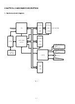
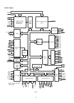
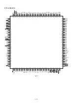
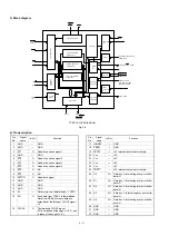
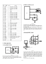
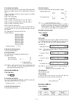
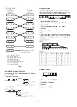
3. Clock generator
1) CPU (HD64151010FX)
Fig. 3-1
Basic clock is supplied from a 19.66 MHz ceramic oscillator.
The CPU contains an oscillation circuit from which the basic clock is
internally driven. If the CPU was not operating properly, the signal
does not appear on this line in most cases.
2) CKDC8 oscillation circuit
Fig. 3-2
Two oscillators are connected to the CKDC8.
The main clock X1 generates 4.19MHz which is used during power on.
When power is turned off, the CKDC8 goes into the standby mode and
the main clock stops.
The sub-clock X2 generates 32.768KHz which is primarily used to
update the internal RTC (real time clock). During the standby mode, it
keeps oscillating to update the clock and monitoring the power recov-
ery.
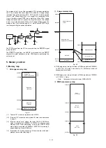
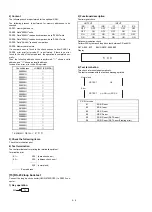
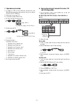
4. Reset (POFF) circuit
Fig. 4-1
In order to prevent memory loss at a time of power off and power
supply failure of the ECR, the power supply condition is monitored at
all times. When a power failure is met, the CPU suspends the execu-
tion of the current program and immediately executes the power-off
program to save the data in the CPU registers in the external S-RAM
with the signal STOP forced low to prepare for the power-off situation.
The signal STOP is supplied to the CKDC8 as signal RESET to reset
the devices.
This circuit mo24V supply voltage.
CPU
(HD64151010FX)
99
98
XTAL
EXTAL
19.66MHz
X4
101
PHAI
37
38
33P
HD404728A91FS
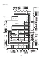
C105
CKDC 8
X2
X1
4.19MHz
X2
32.768KHz
2
1
3
41
18P
C106
40
X1
XT2
XT1
R164
330K
+
-
/POFF
3
2
1
4
8
B
IC7A
KIA393F
C37
1000P
D7
1SS133
C83
1µ 50V
+
ZD2
MTZ5.1A
R116
9.1KG
R115
15KG
R118
56K
R117
2.7K
R119
2.7K
R114
8.2KG
+24V
+5V
POFF
CPU
72
IRQ0
89
RESET (FROM CKDC 8)
STOP (TO CKDC 8)
MPCA7
13
48
1
IR
Q0
54
IN
T0
4 – 13
Summary of Contents for ER-A450
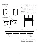
Page 51: ...MAIN PWB LAYOUT 1 SIDE A 8 15 ...
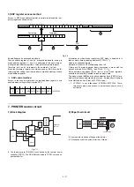
Page 52: ... 2 SIDE B 8 16 ...
Page 53: ...PS PWB FRONT DISPLAY PWB POP UP DISPLAY PWB 8 17 ...