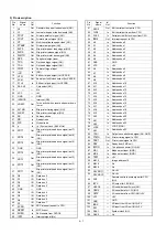
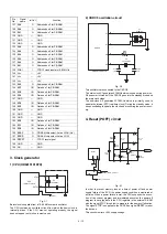
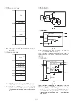


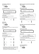
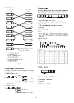
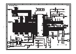


3) SSP register access method
Access to SSP break address register is performed through the tem-
porary register as shown below:
Fig. 6-5
Enable flags can be accessed individually.
Though enable register
4
can be accessed individually, writing to
brake address registers
1
and
2
is performed at the same time as
writing to brake address register
3
through the temporary register.
Therefore, set
1
and
2
to temporary, then write into
3
at last.
Since the temporary register is commonly used by BAR sets, thefol-
lowing register setting is performed after completion ofsetting of each
break address register.
3
SSP control method
Access to the enable register and the brake address register is only
possible when writing to them from the CPU.
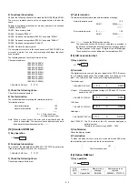
Information on which brake register the SSP brake is detected in is
read as binary data by reading address FFFFFFH (*1).
Used in an expanded register.
Normally is a reserve bit. Whenreading, fixed to 0.
If there are 32 break registers, binary expression is made with the
above 5 bits, and 0th is “00000
B
” and 31st is “11111
B
.”
When detected simultaneously by two or more break registers,
onewith the smaller BAR number is read as binary data.
The brake signals (NMI) and the above detection data (CMP0~4) are-
held until the above detection data are read. So read should bemade
in the NMI sub routine. (Clear by FFFFFFH read.)
*
1: FFFFFFH is not fulldecoded. (FFFF00H~FFFFFFH). There-
fore,unnecessary read access in parentheses should not be
performed.
1
2
3
4
A19 A18 A17 A16 A15
A8
A7
A2
EN
WR
WR
Temporary
Temporary
bit 7
6
5
4
3
2
1
0
0
0
CMP4
0
CMP3 CMP2 CMP1 CMP0 (FFFFFFH)
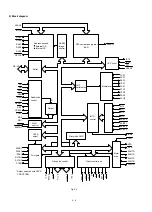
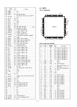
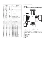
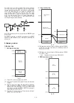
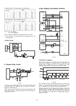
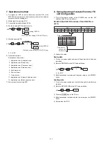
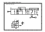
7. PRINTER control circuit
1) Block diagram
Fig. 7-1
·
The thermal printer (PR-45M) is controlled by the thermal printer
controller (TPRC1). The PB-RAM connected to TPRC1 serves as a
print data buffer.
2) Paper feed circuit
·
A pulse motor is used as the paper feed motor.
·
Drive sequence of the pulse motor is as follows:
Address bus
Data bus
CPU
TPRC1
MPCA7
P.B-
RAM
RECEIVER
DRIVER
PRINTER
(PR-45)
RPFC/JPFC
RPFB/JPFB
4AC16
RPPD/JPFD
B
A
C
D
M
RPFA/JPFA
VRCOM/VJCOM
TPRC1
RAS/JAS
RBS/JBS
RCS/JCS
RDS/JDS
4 – 17
Summary of Contents for ER-A450
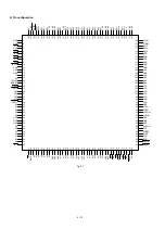
Page 51: ...MAIN PWB LAYOUT 1 SIDE A 8 15 ...
Page 52: ... 2 SIDE B 8 16 ...
Page 53: ...PS PWB FRONT DISPLAY PWB POP UP DISPLAY PWB 8 17 ...