
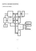
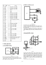


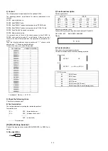
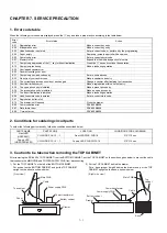

The voltage at the (–) pin of the comparator IC7A is always maintained
to 5.1V by means of the zener diode ZD2, while +24V supply voltage
is divided through the resistors R114, R115 and R116, and is applied
to the (+) pin. When 24V is in supply, 6.8V is supplied to the
(+) pin, therefore, signal POFF is at a high level. When +24V supply
voltage decreases due to a power off or any other reason, the voltage
at the (+) pin also decreases. When +24V supply voltage drops, the
voltage at the (+) pin drops below +5.1V, which causes POFF to go
low, thus predicting the power-off situation.
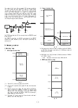
The STOP signal from the CPU is converted into the RESETS signal
by the CKDC8.
The RESETS signal from the CKDC8 is converted into the RESET
signal at the gate backed-up by the VRAM power, performing the
system reset.
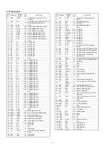
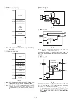
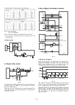
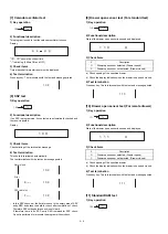
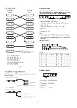
5. Memory control
1) Memory map
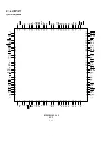
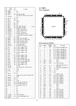
1
All range memory map
Fig. 5-1
(
*
1) “Internal I/O” means the registers in the H8/510.
(
*
2) “External I/O” means the base system I/O area to be addressed
in page 0.
(
*
3) "Memory image area" means the lower 32KB of ROM area
which is projected to 000000H ~ 007FFFH for allowing reset
start and other vector addressing, or the lower 32KB of ROM
area which is projected to 008000H ~ 00FE7FH for allowing 0
page addressing of work RAM area.
(
*
4) “Expansion I/O” means expansion I/O device area which isad-
dressed to area other than page 0.
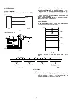
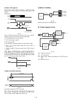
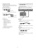
2
0 page memory map
Fig. 5-2
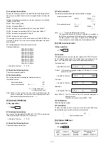
·
ROM image area: Image is formed in ROM area address C00000H
to C07FFFH. This area is identical to IPL ROM area which will
beseparately developed.
·
RAM image area: Image is formed in RAM area address 1F0000H
to 1F7E7FH. (
*
Note)
*
Note:
Image can be formed in lower 32KB of RAS2.
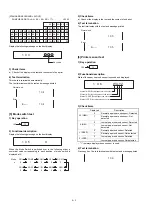
3
ROM area memory map
Fig. 5-3
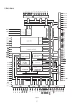
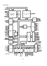
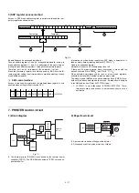
RESETS
STOP
CKDC8
RAS3
4
5
6
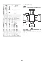
IC12B
74HC00S
/(RAS3./RESET)
/RESET
1
2
3
IC12A
74HC00S
VDD
C86
1000P
C175
1000P
R245
10K
C188
1000P
9
10
8
14
IC12C
74HC00S
14
14
VDD
VDD
Internal I/O
External I/O
Memory image area
(*1)
(*2)
(*3)
RAM area
(10M byte)
ROM area
(3M byte)
Expansion I/O area (1M byte)
000000H
1C0000H
C00000H
FFFFFFH
000000H
004000H
008000H
00FFFFH
1FFFFFH
ROM image area
32KB
RAM image area
slightly smaller than32KB
NOT USE
00F800H
00FE80H
00FF80H
00FFFFH
RAM image area
Internal I/O area
External I/O area
(0 page)
1BFFFFH
RAM area
C00000H
D00000H
EFFFFFH
ROS3
NOT USE
ROS1
(512K Byte)
C80000H
CA0000H
ROS2
(Not used)
4 – 14
Summary of Contents for ER-A450
Page 51: ...MAIN PWB LAYOUT 1 SIDE A 8 15 ...
Page 52: ... 2 SIDE B 8 16 ...
Page 53: ...PS PWB FRONT DISPLAY PWB POP UP DISPLAY PWB 8 17 ...