


This Document can not be used without Samsung’s authorization
Samsung Electronics
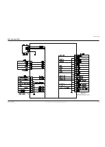
10-1
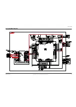
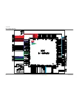
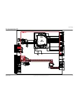
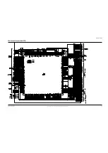
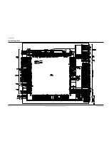
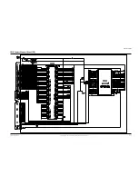
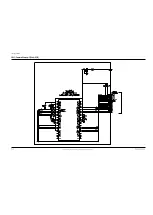
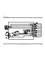
10. Schematic Diagrams
10-1 DC/DC Converter (Main PCB) - - - - - - - - - - - - - - - - - - - - - - - - - - - - - - - - 10-2
10-2 Servo (Main PCB) - - - - - - - - - - - - - - - - - - - - - - - - - - - - - - - - - - - - - - - - 10-3
10-3 System Control (Main PCB) - - - - - - - - - - - - - - - - - - - - - - - - - - - - - - - - - 10-4
10-4 Pre Amp/PRML (Main PCB) - - - - - - - - - - - - - - - - - - - - - - - - - - - - - - - - - 10-5
10-5 DV-1Chip (Main PCB) - - - - - - - - - - - - - - - - - - - - - - - - - - - - - - - - - - - - - 10-6
10-6 Video-Interface (Main PCB) - - - - - - - - - - - - - - - - - - - - - - - - - - - - - - - - - 10-7
10-7 Audio (Main PCB) - - - - - - - - - - - - - - - - - - - - - - - - - - - - - - - - - - - - - - - - 10-8
10-8 Camera Process (Main PCB) - - - - - - - - - - - - - - - - - - - - - - - - - - - - - - - - 10-9
10-9 DSP (Main PCB) - - - - - - - - - - - - - - - - - - - - - - - - - - - - - - - - - - - - - - - - - 10-10
10-10 Camera Memory 1 (Main PCB) - - - - - - - - - - - - - - - - - - - - - - - - - - - - - - 10-11
10-11 Camera Memory 2 (Main PCB) - - - - - - - - - - - - - - - - - - - - - - - - - - - - - - 10-12
10-12 CCD (CCD PCB) - - - - - - - - - - - - - - - - - - - - - - - - - - - - - - - - - - - - - - - - - 10-13
10-13 Front (Front PCB)- - - - - - - - - - - - - - - - - - - - - - - - - - - - - - - - - - - - - - - - 10-14
10-14 Jack (Jack PCB) - - - - - - - - - - - - - - - - - - - - - - - - - - - - - - - - - - - - - - - - 10-15
10-15 Rear (Rear PCB) - - - - - - - - - - - - - - - - - - - - - - - - - - - - - - - - - - - - - - - - 10-16
10-16 Function (Function PCB)- - - - - - - - - - - - - - - - - - - - - - - - - - - - - - - - - - - 10-17
10-17 CVF (CVF PCB) - - - - - - - - - - - - - - - - - - - - - - - - - - - - - - - - - - - - - - - - - 10-18
10-18 LCD (LCD PCB) - - - - - - - - - - - - - - - - - - - - - - - - - - - - - - - - - - - - - - - - - 10-19
For schematic Diagram
- Resistors are in ohms, 1/8W unless otherwise noted.
Note
Special note :
Most semiconductor devices are electrostatically sensitive and therefore require the special handling techniques described under the
“electrostatically sensitive (ES) devices” section of this service manual.
Note :
Do not use the part number shown on this drawing for ordering. The correct part number is shown in the parts list (may be slightly
different or amended since this drawing was prepared).
Important safety notices :
Components identified with the mark have the special characteristics for safety. When replacing any of these components.
Use only the same type.
Page
Summary of Contents for VP-D455
Page 10: ...Product Specification 2 4 Samsung Electronics MEMO...
Page 30: ...3 20 Alignment and Adjustments Samsung Electronics MEMO...
Page 46: ...4 16 Disassembly and Reassembly Samsung Electronics MEMO...
Page 66: ...Exploded View and Parts List 5 20 Samsung Electronics MEMO...
Page 83: ...Samsung Electronics 8 1 8 Wiring Diagram MEMORY STICK VP D453 I D6620I VP D454 I D455 I D6650I...
Page 84: ...Wiring Diagram 8 2 Samsung Electronics MEMO...
Page 86: ...PCB Diagrams 9 2 Samsung Electronics 9 1 Main PCB COMPONENT SIDE...
Page 87: ...PCB Diagrams Samsung Electronics 9 3 L708 L704 L706 L717 L719...
Page 88: ...PCB Diagrams 9 4 Samsung Electronics CONDUCTOR SIDE Fuse 1 25A 32V...
Page 94: ...PCB Diagrams 9 10 Samsung Electronics MEMO...
Page 128: ...Troubleshooting 12 8 Samsung Electronics MEMO...
Page 140: ...Circuit Operating Description 13 12 Samsung Electronics MEMO...
Page 184: ...Reference Information 14 44 Samsung Electronics MEMO...