3-22
CIRCUIT DESCRIPTION
Samsung Electronics
Repair Manual
CS
RD
VVR
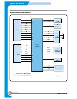
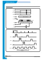
A0/ALE
D[7:0]/AD[7:0]
INTR
MODE[1:0]
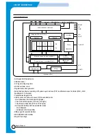
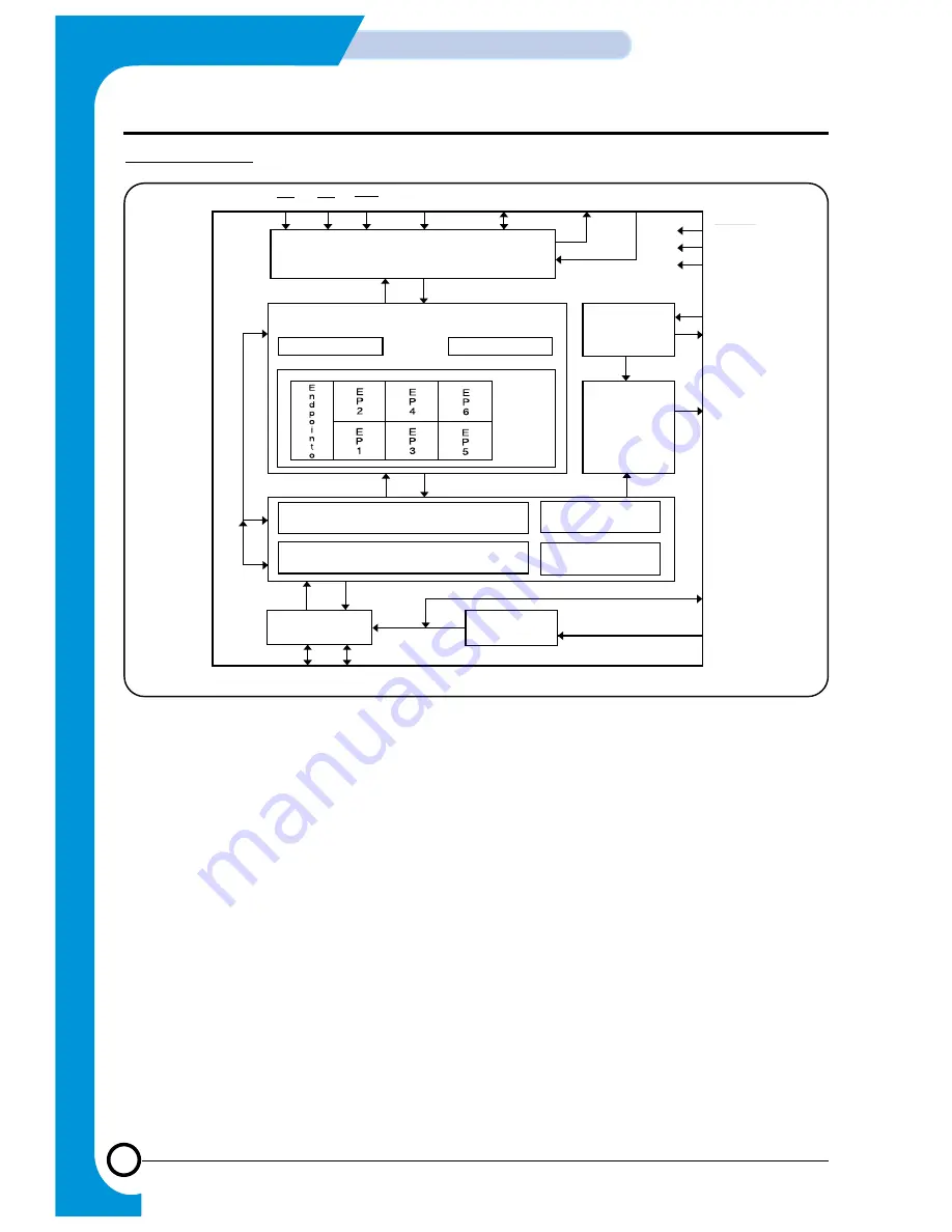
Microcontroller Interface
Endpoint/Contol FIFOs
Control
Status
RX
TX
RESET
Vcc
GND
XIN
XOUT
CLKOUT
48 MHz
Oscillator
Clock
Generator
SIE
Media Access Controller[MAC]
Physical Layer interface[PHY]
Trans ceiver
VReg
Clock
Recovery
USB Event
Detect
V3.3
AGND
D+
D-
Upstream Port
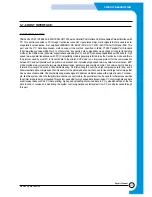
USB INTERFACE
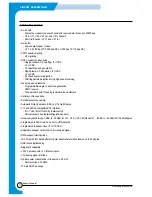
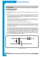
• Full-Speed USB Node Device
• USB transceiver
• 3.3V signal voltage regulator
• 48 MHz oscillator circuit
• Programmable clock generator
• Serial Interface Engine consisting of Physical Layer In-terrace (PHY) and Media Access Controller (MAC), USB
Specification 1.0 compliant
• Control/Status Register File
• USB Function Controller with seven FIFO-based End-points :
- One bidirectional Control Endpoint 0 (8bytes)
- Three Transmit Endpoints (2*32 and 1*64 bytes)
- Three Receive Endpoints (2*32 and 1*64 bytes)
• 8-bit parallel interface with two selectable modes :
- non-multiplexed
- multiplexed (Inter compatible)
• DMA support for parallel interface
• MICROWIRE/PLUS Interface
• 28-pin SO package
Summary of Contents for SF-530 Series
Page 87: ...Electronics ...

