3-6
CIRCUIT DESCRIPTION
Samsung Electronics
Repair Manual
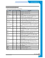
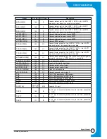
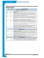
Signal
Pin No.
I/O Type
Description
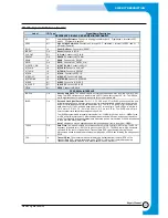
nECS[1:0]
12,13
O1
Not external chip select. Three I/O banks are provided for
external memory-mapped I/O operations. Each I/O bank
contains up to 4M half-word. The nECS signals indicate that
an external I/O bank is selected.
nRCS[2]
51
O2
Not ROM/SRAM chip select. The KS32C65100 can access
up to three external ROM/SRAM banks. nRCS[0]
corresponds to ROM/SRAM bank 0, nRCS[1] to bank 1, and
nRCS[2] to bank 2. By controlling the nRCS signals, CPU
addresses can be mapped into the physical memory banks.
nRCS[1]/GOPA[7]
50
O1
nRCS[0]
49
O1
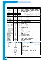
SC_CONPHA/
GOPA[19]
102
O1
Scan motor control/Bi-phase
SC_CONPHB/
GOPA[20]
105
O1
Scan motor control/Bi-phase
SC_CUR[3:0]
103, 104,
106, 107
O1
Scan motor bi-current/uni-phase
PWM O[2:0]/
GOPA[13:11]
118~120
O1
PWM out signal
VDO2/GOPA[29]
121
O4
Video out from PIFC
VDO1/GOPA[14]
122
O5
Video out from LSU control
LSU_CLK/
GOPA[15]
123
O1
Clock for LSU motor
nHSYNC1/GIP[10]
125
I1
HSYNC1
nLREADY/GIP[11]
126
I1
LSU ready
nHSYNC2/GIP[12]
127
I1
HSYNC2
VDI/GIP[13]
128
I2
Video data input from RET
VCLK/GIP[14]
129
I2
External video clock
nEXTWAIT/GIP[7]
130
I3
External wait
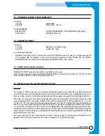
RTCXIN
202
I7
RTC oscillator clock input.
RTCXOUT
203
O7
RTC oscillator clock output.
SLED[2:0]/
GOPA[18:16]
196~198
O1
CIS LED signals
GAVRT
205
I5
Top reference voltage for general ADC
GAIN[2:0]
206~208
I5
Analog inputs for general ADC
RTC_VDD
201
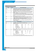
RTC VDD.
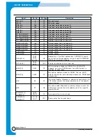
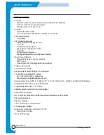
Signal
Pin No.
I/O Type
Description
VDD_PLL
186
PLL power (3.3V).
SAVDD
1
Analog power for scan ADC and general ADC (3.3V).
SAVSS
5
Scan ADC ground.
GAVSS
204
General ADC ground
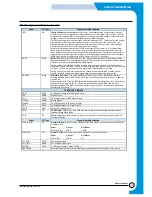
3VDD
15, 30, 81,
115, 131,
160
3.3V internal power.
Externally connected to the 3.3V regulator.
5VDD
48, 67, 89,
141, 195
5V I/O power.
Externally connected to the VCC board plane.
VSS
11, 25, 39,
58, 76, 101,
108, 124,
150, 172,
181
System ground.
Externally connected to the ground board plane.
Summary of Contents for SF-530 Series
Page 87: ...Electronics ...

