3-4
CIRCUIT DESCRIPTION
Samsung Electronics
Repair Manual
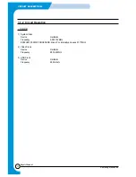
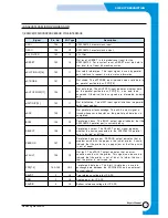
Signal
Pin No.
I/O Type
Description
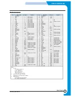
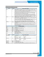
CIS_CLK
6
O1
CIS shift clock
CIS_SI
7
O1
CIS latch signal
PHA_IA0
164
O1
Line feed motor phase signal A
PHA_IA1
165
O1
Line feed motor phase signal AZ
PHB_IB0
167
O1
Line feed motor phase signal B
PHB_IB1
168
O1
Line feed motor phase signal BZ
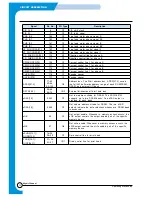
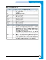
LF_PH0/GOPA[21]
163
O1
Line feed motor control signal 0
LF_PH1/GOPA[22]
166
O1
Line feed motor control signal 1
CR_PHA/GOPA[23]
110
O1
Direction control line for phase A
CR_PHB/GOPA[24]
113
O1
Direction control line for phase B
CRIA0/GOPA[25]
109
O1
Current control line 0 for phase A
CRIA1/GOPA[26]
111
O1
Current control line 1 for phase A
CRIB0/GOPA[27]
112
O1
Current control line 0 for phase B
CRIB1/GOPA[28]
114
O1
Current control line 1 for phase B
CHX/GIP[8]
116
I3
Encode sensor
CHY/GIP[9]
117
I3
Encode sensor
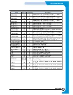
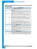
ADDR[21:0]
77~80,
82~88,
90~100
O5
Address bus. The 22bit address bus, ADDR[21:0], covers
the full 4M half-words address range of each ROM/SRAM,
DRAM, and external I/O bank
DATA[15:0]
59~66,
68~75
I/O3
External bi-directional 16-bit data bus.
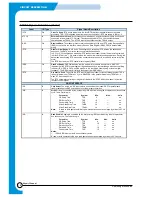
nRAS[1:0]
52,53
O1
Not row address strobe for DRAM. The KS32C65100
supports up to two DRAM banks. One nRAS output is
provided for each bank.
nCAS[1:0]
54,55
O1
Not column address strobe for DRAM. The two nCAS
outputs indicate the byte selections whenever a DRAM bank
is accessed.
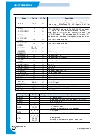
nOE
56
O1
Not output enable. Whenever a memory access occurs, the
nOE output controls the output enable port of the specific
memory device.
nWE
57
O6
Not write enable. Whenever a memory access occurs, the
nWE output controls the write enable port of the specific
memory device.
nPHGA[13:1]/
GOPB[12:0]
16~24,
26~29
O1
Gate control line for print head.
PHOE[16:1]/
GIOP[26:11]
31~38,
40~47
I/O1
Drain control line for print head.
Summary of Contents for SF-530 Series
Page 87: ...Electronics ...

