Circuit Descriptions, List of Abbreviations, and IC Data Sheets
EN 92
F21RE AB
9.
The AVI contains a video switch, an audio switch, an I/O
expander, and an EPLD (or ACEX) with I2C control.
The AVI panel is an interface between the following panels/
sources:
•
Small Signal panel (SSP).
•
Front panel (FP).
•
VGA input.
•
Standard Definition panel (SD).
•
Power Supply panel (PS).
It also contains the outputs to the plasma monitor.
9.3.2
AVI: Video Processing
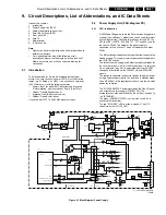
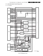
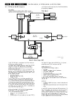
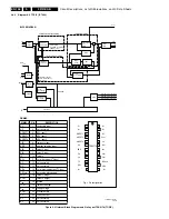
Figure 9-5 Block diagram video processing
1fH CVBS and YC Video Selection (diagram AV7)
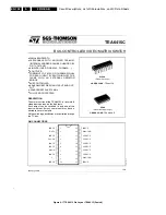
For the video source selection, a TEA6415 (item 7710) from
SGS-Thomson is used. The main function of this IC is to switch
eight video input sources to six outputs. Each output can be
switched to only one of the inputs, but any same input may be
connected to several outputs. All the switching possibilities are
controlled through the I2C bus.
At the input of the IC, we find the following signals:
•
CVBS or Y/C from FRONT.
•
CVBS or Y/C from EXT3.
•
CVBS or Y/C from the Scaler (not used in this chassis).
At the output of the IC we find:
•
CVBS_Y_AV1 and C_AV1.
•
CVBS_Y_AV2 and C_AV2.
AV1 is connected to the CVBS/YC_FRONT input of the SSP
(connector 0333).
AV2 is connected to the CVBS/YC_UI input of the SSP
(connector 0372).
These signals go to the SSP via connectors 0333 and 0372,
where they are fed to a second TEA6415 (item 7208), together
with the video signals coming from the SCART connectors.
1fH Video processing (diagram AV6)
The YPbPr signals coming from the SD panel (EXT5) are
buffered, and then fed through a YPbPr-to-RGB matrix circuit
(TSH93, item 7607). The matrix is made with discrete hardware
and determined by resistor values.
The RGB_SD output signals are then fed to connector 0372
and routed, via an RGB selector, to the RGB2 (Universal
Interface) input of the HIP IC (item 7501) on the SSP.
9.3.3
AVI: Sync Processing
General
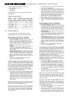
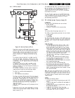
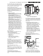
Figure 9-6 Block diagram sync processing
The block diagram above shows the sync path. The AV
Interface has the following sync inputs:
•
Sync from VGA source (HV_VGA)
•
Sync from SSP (HD_VD)
The selection between these inputs for the main picture is done
with switch 7570. This switch is controlled via software with the
HD_VGA_SELECT signal.
Note: If the Receiver box has to function without the monitor
(e.g. in case of EPG data download), the H and V pulses may
not be fed to the monitor. In this case, switch 7570 will be put
open with the SYNC_TRISATE_MON control signal (SW
controlled).
9.3.4
AVI: Audio Processing
General
The audio-part of the AV-interface consists of three separate
parts:
•
The source selection.
•
The Channel-channel configuration.
•
Muting (or anti-plop circuit).
Source Selection
The source selection part redirects the three stereo inputs into
two separate channels. These two channels (SNDL/
R_MAIN_OUT and SNDL/R_SUB_OUT) are then connected
to the SSP for further processing.
Note: The TEA6422 cannot handle the maximum level of 2.8 V
of the SNDL/R_VGA signals. Therefore, these signals are
attenuated by 3 dB (see R3801/3802 and R3806/3807 on
diagram AV8). All other inputs are attenuated at the Front I/O
panel or the HD connector panel. These attenuations are
corrected again on the SSP.
Centre Channel Selection
The Centre input (cinch at the rear) is a separate audio input.
This input bypasses all other inputs, and is designed to obtain
a better Home Cinema configuration. In this case, the FTV
monitor speakers will function as the centre channel. This input
is selected via the CENTER_SELECT signal, which is
controlled by the I/O Expander (items IC7880 and TS7853). It
is selected by the user from the user menu.
Mute
To prevent audio plops and clicks (when the set is turned "on/
off" or at channel switching), a mute circuit is implemented
immediately after the centre channel selection part.
YPbPr to
YUV (RGB)
CL36532030_013.eps
030403
VGA
input
HOP
FBX
HIP
Tuner
SSP
TEA 6415
TEA 6415
I/O
IF
SubD
15p
RGB_VGA
AV
INTERFACE
TO PDP
MONITOR
RGB_VGA
RGB_HD
7300
7501
1101
RGB_VC
7208
SD-
panel
front-
panel
CVBS/Y C
CVBS_Y_AV1
& C_AV1
ANTENNA
SCART1
SCART2
CVBS/YC
SCART4
RGB-Fbl_1fH
YUVFbl_1fH_sc1_in
CVBS_Y_AV2
& C_AV2
YPbPr 1fH
SubD
15p
VGA
OUTPUT
RGB_MON
AV7
AV6
FP
SD
AV
K
V_HD
H_HD
(N.C. for Europe)
VD
HD_VGA-SELECT (from OTC)
SYNC_TRISTATE_MON (from OTC)
HD
(from SSP)
H
V
VGAin
H
V
H_MON
V_MON
7575
7570
7450
H_HD_VGA
V_HD_VGA
H_VGA
V_VGA
VGAout
BUFFERS
CL 16532023_055.eps
240901
Summary of Contents for F21RE
Page 7: ...Directions for Use EN 7 F21RE AB 3 3 Directions for Use ...
Page 8: ...Directions for Use EN 8 F21RE AB 3 ...
Page 9: ...Directions for Use EN 9 F21RE AB 3 ...
Page 10: ...Directions for Use EN 10 F21RE AB 3 ...
Page 11: ...Directions for Use EN 11 F21RE AB 3 ...
Page 12: ...Directions for Use EN 12 F21RE AB 3 ...
Page 13: ...Directions for Use EN 13 F21RE AB 3 ...
Page 14: ...Directions for Use EN 14 F21RE AB 3 ...
Page 15: ...Directions for Use EN 15 F21RE AB 3 ...
Page 16: ...Directions for Use EN 16 F21RE AB 3 ...
Page 17: ...Directions for Use EN 17 F21RE AB 3 ...
Page 18: ...Directions for Use EN 18 F21RE AB 3 ...
Page 19: ...Directions for Use EN 19 F21RE AB 3 ...
Page 20: ...Directions for Use EN 20 F21RE AB 3 ...
Page 21: ...Directions for Use EN 21 F21RE AB 3 ...
Page 22: ...Directions for Use EN 22 F21RE AB 3 ...
Page 23: ...Directions for Use EN 23 F21RE AB 3 ...
Page 24: ...Directions for Use EN 24 F21RE AB 3 ...
Page 25: ......
Page 114: ...Revision List EN 114 F21RE AB 11 11 Revision List First release ...


