Circuit Descriptions, List of Abbreviations, and IC Data Sheets
EN 90
F21RE AB
9.
Regulation is performed by the control loop that consists of
reference component 7011 and optocoupler 7002. When the
+5V2 output voltage rises, the reference voltage on the TL431
will exceed 2.5 V and the current through this device and the
optocoupler LED will increase. By this method, the optocoupler
transistor will conduct more, and the voltage over R3035 (and
pin 14 of IC7001) will rise. The IC will adjust the duty cycle, the
FET will conduct less, and the output voltage will decrease.
Protections
Soft Start and Maximum Duty Cycle
The output voltage is 0 V at start up. This would force IC 7001
to start with a maximum duty cycle, causing a very high current
through FET 7000. To prevent this, capacitor C2018 (at pin 11
of IC7001) ensures a soft start (voltage at pin 11 is low at start
up, which gives a small duty cycle) and R3039 determines the
maximum duty cycle.
Switch Off Peak Voltage
To protect the FET against high peak (drain-source) voltages
at switch "off", a peak clamp circuit is added consisting of
D6014, D6002, C2007, and R3010.
When the FET blocks, the diodes will lead the peak voltages
away from the FET and will charge C2007.
When the FET conducts, this capacitor is discharged via
R3010, the primary coil, and the FET itself.
Over Current and Fold Back
The current through the primary winding is measured by sense
resistors R3012, R3013, and R3014. The resulting voltage is
measured at pin 7 of IC7001. Once the voltage at this pin
exceeds 1 V (so maximum current is set to 3 A), the duty cycle
is regulated back.
If the output load keeps on increasing (I > 3 A), the system is
unable to supply enough energy to maintain the output voltage
in regulation. This is detected at pin 5 of IC7001 (via pin 8 of
5003, R3015, D6007 and R3037). Consequently, if this voltage
drops below the fold back threshold voltage of 1 V, the IC will
adapt the "current sense threshold". This will limit the current
supply and by this, the output voltage. This will cause an
avalanche effect, causing the supply to rapidly trim down.
Over Voltage
When the voltage on pin 6 of IC7001 will exceed 2.5 V, the
control IC will stop oscillating (after 2
µ
s). The output voltages
will drop, and the IC starts again. This can happen when the
feedback loop is interrupted.
Demagnetisation
The internal demagnetisation block in IC7001 disables the
output (pin 3) during the demagnetisation phase of transformer
5003. This is to prevent the FET from being switched "on". The
info is taken from pin 8 of transformer 5003, and fed via R3015
and R3030 to pin 8 of IC7001. When the voltage on this pin
drops below 65 mV, the demagnetisation phase is completed,
and the FET can switch on.
Audio Plop
The POWER_VALID circuit is designed to detect the
disappearance of the Mains voltage (at set switch "off" or at
Mains voltage dips). This signal will then mute the audio
outputs to prevent audio plops (see diagram AV8 position I7).
The circuit compares the +5V2 output with the negative
rectified 5V2 winding (which is in fact the transformed rectified
Mains voltage). When this voltage disappears, transistor 7101
is activated and the POWER_VALID output will go "low" before
the supply output voltages will drop. It will mute the audio
outputs and stay "low" until the Mains voltage and the +5V2
output voltage returns.
Switch On/Off Behaviour
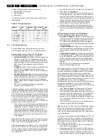
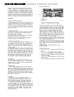
Figure 9-3 Timing diagram Power Supply
The start up of the PSU has to fulfil certain requirements.
At the moment the Mains cord is connected (t0), the standby
supply will generate the +5VSTBY (coming from the STANDBY
pre-condition). With this voltage present, the microprocessor
begins the start up procedure, by making the STANDBY
command logic "low" (t1) and the POWER_ON command
"high" (coming from the "off" pre-condition). After you press the
power switch on the front panel, the "POWER_ON" signal will
become "high" and within 2 seconds, the main supply will start,
making the POWER_VALID signal "high" (t2).
When a Mains dip occurs (t3), the POWER_VALID signal must
go "low" before the output voltages will drop and must remain
"low" until the Mains voltage returns.
When you put the set in standby, the microprocessor makes
the STANDBY signal "high" (t7). The output voltages will drop,
and the POWER_VALID signal goes "low", but the +5VSTDBY
remains present.
Finally, this voltage will drop when the Mains cord is
disconnected (t10).
Typical timing values are:
•
t1 - t2 = 0.1 < t < 1.2 s (dependent on the STANDBY PSU
load).
•
t3 - t4 = 20 < t < 350 ms (dependent on U_MAINS).
•
t4 - t5 = 5 < t < 40 ms (dependent on the main PSU load).
•
t5 - t6 = 10 < t < 1000 ms (dependent on U_MAINS and the
STANDBY PSU load).
•
t7 - t8 = 10 < t < 600 ms (dependent on U_MAINS and the
MAIN PSU load).
•
t8 - t9 = 5 < t < 40 ms (dependent on the MAIN PSU load).
CL16532098_002.eps
240901
t0
t0
t1
t3
t7
t10
= Mainsplug In.
= From STANDBY to ON.
Mainsplug In
Mainsplug Out
Mains Dip
STBY to ON
ON to STBY
= Mainsdip
= From ON to STANDBY
= Mainsplug Out
Umains
5Vstby
Standby
33V, 8V6, 7V7, 5V2, -7V7
Power_valid
t6
t10
t9
t8
t7
t5
t4
t3
t2
t1
Summary of Contents for F21RE
Page 7: ...Directions for Use EN 7 F21RE AB 3 3 Directions for Use ...
Page 8: ...Directions for Use EN 8 F21RE AB 3 ...
Page 9: ...Directions for Use EN 9 F21RE AB 3 ...
Page 10: ...Directions for Use EN 10 F21RE AB 3 ...
Page 11: ...Directions for Use EN 11 F21RE AB 3 ...
Page 12: ...Directions for Use EN 12 F21RE AB 3 ...
Page 13: ...Directions for Use EN 13 F21RE AB 3 ...
Page 14: ...Directions for Use EN 14 F21RE AB 3 ...
Page 15: ...Directions for Use EN 15 F21RE AB 3 ...
Page 16: ...Directions for Use EN 16 F21RE AB 3 ...
Page 17: ...Directions for Use EN 17 F21RE AB 3 ...
Page 18: ...Directions for Use EN 18 F21RE AB 3 ...
Page 19: ...Directions for Use EN 19 F21RE AB 3 ...
Page 20: ...Directions for Use EN 20 F21RE AB 3 ...
Page 21: ...Directions for Use EN 21 F21RE AB 3 ...
Page 22: ...Directions for Use EN 22 F21RE AB 3 ...
Page 23: ...Directions for Use EN 23 F21RE AB 3 ...
Page 24: ...Directions for Use EN 24 F21RE AB 3 ...
Page 25: ......
Page 114: ...Revision List EN 114 F21RE AB 11 11 Revision List First release ...


