


MSC711x Application Development System (MSC711xADS) Reference Manual, Rev. 1
48
Freescale Semiconductor
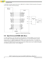
MSC711xADS Interfaces
5.8.2
SDRAM Refresh
The SDRAM is refreshed in its auto-refresh mode. Using the SDRAM machine 1 periodic timer, an auto-refresh
command is issued to the SDRAM every 8.2 µsec so that all 4096 SDRAM rows are refreshed within the specified
34 msec. An interval of ~30 msec of refresh redundancy within that window is a safety measure to cover for
possible delays in bus availability for the refresh controller.
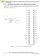
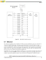
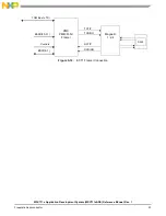
5.9 Flash Memory
The MSC711xADS has an 8 MB (4 M at 16) Flash memory that is implemented using the AM29LV641DL120
from AMD. The Flash memory is buffered from the 60x bus to reduce its capacitive load. To minimize use of
MPC8272 chip-select lines, only one chip-select line (
CS0
) is used to select the Flash memory. Flash memory can
be disabled(1) or enabled (0) at any time by writing to the FlashEn bit in BCSR1. Figure 5-10 shows the Flash
memory connection scheme
.
The access time of the MSC711xADS Flash memory unit is 90 ns. However, Flash memories with different delay
times are supported as well. Flash memory is controlled with the GPCM and a dedicated
CS0
region that controls
the whole bank.
Figure 5-10. Flash Memory Connection Scheme
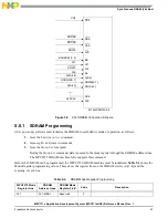
SDA10
A10
Opcode
0
A19
A9
Reserved
0/1
0
Burst read and burst write (copy-back data
cache).
1
Burst read and single write (write-through data
cache).
A20
A8
Reserved
0
A21
A7
Reserved
0
A[22–24]
A[6–4]
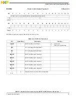
CAS Latency
011
Data valid 3 clock cycles after CAS asserted.
A25
A3
Burst Type
0
Sequential burst.
A[26–28]
A[2–0]
Burst Length
010
4 operand burst length.
Table 5-3. DRAM Mode Register Programming (Continued)
MPC8272 Mode
Register Line
SDRAM
Address Linea
SDRAM Mode
Register Field
Value
Description
CS0
D[15–0]
Flash Memory
D[0–15]
A[9–30]
WE0
POE
CS0
POE
WE0
A[22–0]