
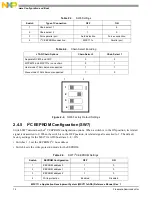


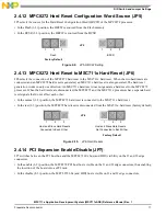
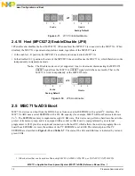


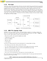
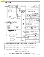


MSC711xADS Boot
MSC711x Application Development System (MSC711xADS) Reference Manual, Rev. 1
Freescale Semiconductor
19
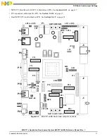
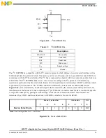
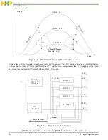
Figure 2-13. I
2
C EEPROM Pins
The I
2
C EEPROM is compatible with the I
2
C memory protocol, which defines a two-wire serial interface with a
bidirectional data bus and serial clock. The memory carries a 4-bit unique device type identifier code (0b1010) in
accordance with the I
2
C bus definition. The I
2
C bus is connected to a header with two test points, and its clock runs
at 400 KHz. The I
2
C EEPROM behaves as a slave device according to the I
2
C protocol, with all memory
operations synchronized by the serial clock. Read and write operations are initiated by a START condition, which
is generated by the bus master. The START condition is followed by a device select code and RW bit (see
Figure 2-14). It is terminated by an acknowledge bit that is inserted by the memory immediately after the 8-bit
transmission of the bus master, thus comprising a 9
th
bit. When the bus master reads the data, it acknowledges the
receipt of the data byte by placing an acknowledge 9
th
bit into the transmission stream. Data transfers are
terminated by a STOP condition after an Ack for WRITE, and after a No Ack for READ.
.
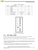
Figure 2-14. Device Select Code
Table 2-7. I
2
C EEPROM Pins
Pin
Description
E0, E1, E2
Chip enable
SDA
Serial data
SCL
Serial clock
WC
Write control
V
CC
Supply voltage
V
SS
Ground
Device Type Identifier
Chip Enable
RW
7
6
5
4
3
2
1
0
Device Select Code
1
0
1
0
0
0
0
RW
Note: The most significant bit, 7, is sent first.
3
V
CC
SDA
E[0–2]
SCL
WC
V
SS