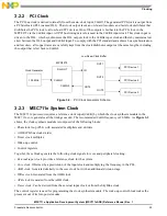
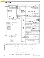

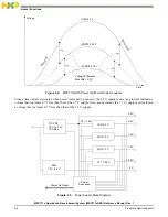


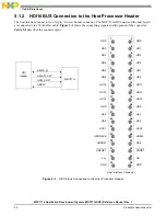


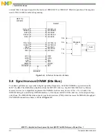


HDI16 Host Processor Interface
MSC711x Application Development System (MSC711xADS) Reference Manual, Rev. 1
Freescale Semiconductor
39
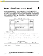
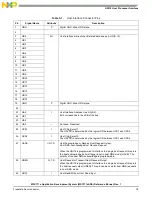
Table 5-1. Host Interface Connector Pins
Pin
Signal Name
Attribute
Description
1
GND
P
Digital GND. Main GND plane.
2
3
HD0
I/O
Host interface bidirectional tri-stated data bus port: HD[0–15].
4
HD1
5
HD2
6
HD3
7
HD4
8
HD5
9
HD6
10
HD7
11
HD8
12
HD9
13
HD10
14
HD11
15
HD12
16
HD13
17
HD14
18
HD15
19
GND
P
Digital GND. Main GND plane.
20
21
HA0
I
Host Interface Address Line HA[0–3].
Bit 0 corresponds to the LSB of the bus.
22
HA1
23
HA2
24
HA3
—
Not used. Reserved.
25
HCS1
I
Host Chip-Select 1.
The HDI CS is determined by the logical OR between HCS1 and HCS2.
26
HCS2
I
Host Chip-Select 2.
The HDI CS is determined by the logical OR between HCS1 and HCS2.
27
HACK
I/O,T.S.
Host Acknowledge or Receive Host Request Output.
Host DMA Acknowledge/Host Receive Request
When the HDI16 is programmed to interface to a single host request, this pin is
the host acknowledge Schmitt trigger input in host DMA mode (HACK). The
polarity of the host DMA acknowledge is programmable.
28
HREQ
Q,T,S
Host Request or Transmit Host Request Output.
When the HDI16 is programmed to interface to a single host request, this pin is
the host request output (HREQ). This pin can be used for host DMA requests
in host DMA mode.
29
HRW
I
Host Read/Write or Host Read Input.