


Clocking
MSC711x Application Development System (MSC711xADS) Reference Manual, Rev. 1
Freescale Semiconductor
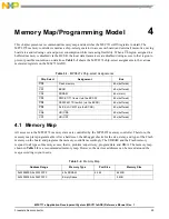
25
3.2.2
PCI Clock
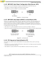
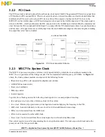
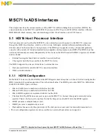
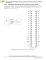
The PCI bus clock is derived internally from the main clock input,
CLKIN1
. The generated PCI clock is output from
a PCI-dedicated PLL (named DLL). That clock output feeds an on-board low-skew and fast clock distributor that
distributes the PCI clock to all on-board PCI devices. One of the outputs is fed back to the PCI clock in the
MPC8272 via the
CLKIN2
input. All PCI bus timings are referenced to the
CLKIN2
input clock. This clock input is
driven to the DLL, which synchronizes the DLL output clock to the
CLKIN2
input clock and thereby maintains low
skew between the DLL output and
CLKIN2
input. To comply with the PCI standard and achieve bus synchronization
and low skew, all copper traces are carefully kept from the clock distributor outputs at the same lengths, including
the output that is fed back to
CLKIN2
.
Figure 3-2. PCI Clock Generator Scheme
3.2.3
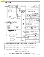
MSC711x System Clock
The MSC711x processor requires a reference clock input (
CLKIN
) by which the clock synthesis module in the
MSC711x core generates all the timings needed. The recommended
CLKIN
frequency is 20 MHz. As Figure 3-3
shows, the clock synthesis module is composed of the following blocks:
• Phase lock loop (PLL) with associated multipliers and dividers
• AHB/APB bus clock divider
• Timer clock multiplex
• Wake-up control
• Control registers
Together, these blocks generate the following clock signals for core and peripheral clocking:
• External input clock. provides a reference clock for the system.
• Core clock. Obtained by a predivision of the input clock and multiplying the frequency in the PLL.
• AHB clock. Generated similarly to the core clock but with an additional division stage.
• IPBus clock. Generated from the AHB clock.
• APB clock. Generated from the AHB clock.
• Timer clock. Can be derived from the external input clock or from the SkyBlue clock.
The control register is used for programming the clock synthesis module. The wake-up control block wakes the
processor out of its low-power modes.
PCI Device 1
PCI Device 2
PCI Device 3
OUT1
OUT2
OUT3
OUT4
IN
Low Skew Clock Buffer
MPC8272
DLLOUT
CLKIN1
CLKIN2
Clock Generator
100 MHz