


DIP-Switch and Jumper Settings
MSC711x Application Development System (MSC711xADS) Reference Manual, Rev. 1
Freescale Semiconductor
17
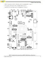
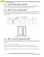
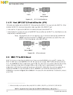
2.4.12 MPC8272 Hard Reset Configuration Word Source (JP5)
JP5 selects the source for the Hard Reset Configuration Word (HRCW) of the MPC8272 processor.
• In the Flash (1-2) position, the HRCW is sourced from the Flash memory.
• In the BCSR (2-3) position, the HRCW is sourced from the BCSR.
Figure 2-9. JP5, HRCW Setting
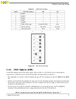
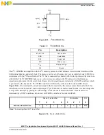
2.4.13 MPC8272 Hard Reset to MSC711x Hard Reset (JP6)
JP6 selects the connection of the MPC8272 hard reset to the MSC711x hard reset. When the two hard resets are
connected and an MPC8272 hard reset is generated, an MSC711x hard reset is also generated. The hard reset
generation works in only one direction. An MSC711x hard reset does not generate a hard reset to the MPC8272
processor. When the hard resets are disconnected, the MPC8272 and the MSC711x processors have separate hard
reset signals that do not affect each other.
• In the normal (1-2) position, the MPC8272 hard reset is connected to the MSC711x hard reset.
• In the test (2-3) position, the MPC8272 hard reset is disconnected from the MSC711x hard reset (factory default)
Figure 2-10. JP6, Hard Resets
2.4.14 PCI Expansion Enable/Disable (JP7)
JP7 switches between the PCI host bus and the MPC8272 60x bus (and HDI) visibility on the J1 and J2 edge
connectors.
• In the enable (1-2) position, the MPC8272 PCI host bus is visible on the J1 and J2 edge connectors, thus enabling
the insertion of the board into a cPCI rack.
• In the disable (2-3) position, the MPC8272 60x (and HDI) bus is visible on J1 and J2 edge connectors.
1
2
3
1
2
3
Flash
Factory Default
BSCR
JP5
1
2
3
1
2
3
Host and Slave Hard Resets
Factory Default
Connected to Each Other
Host and Slave Hard Resets
Not Connected to Each Other
JP6