


MSC711x Application Development System (MSC711xADS) Reference Manual, Rev. 1
32
Freescale Semiconductor
Memory Map/Programming Model
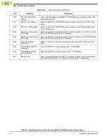
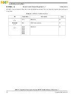
BCSR1 can be read at any time, and it gets its defaults at power-on reset.
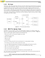
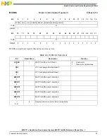
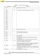
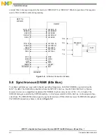
BCSR1
Board Control Status Register 1
Offset 0x4
Bit
0
1
2
3
4
5
6
7
8
9
10
11
12
13
14
15
BVER0 BVER1 PCIEN PCIM66E PCIINTA PCIINTB PCIINTCPCIINTD
TYPE
R
RESET
0
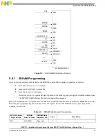
Bit
16
17
18
19
20
21
22
23
24
25
26
27
28
29
30
31
TYPE
R
RESET
0
Table 4-2. BCSR1 Bit Descriptions
Bit
Reset Value
Description
Settings
BVER0
0
0
Board version 0.
00 Prototype.
01
Pilot.
10 Rev.
A.
11 Rev.
B.
BVER1
1
0
Board version 1.
PCIEN
2
0
PCI enable (HDI disable).
0 PCI
connection
enable.
1
60x (HDI) connection enabled.
PCIM66E
3
0
PCI 66 MHz enable.
0
PCI bus is working at 66 MHz.
1
PCI bus is working at 33 MHz.
PCIINTA
4
0
PCI interrupt A.
0 Interrupt.
1 No
interrupt.
PCIINTB
5
0
PCI interrupt B.
0 Interrupt.
1 No
interrupt.
PCIINTC
6
0
PCI interrupt C.
0 Interrupt.
1 No
interrupt.
PCIINTD
7
0
PCI interrupt D.
0 Interrupt.
1 No
interrupt.
—
8–31
0
Reserved. Write to zero for future compatibility.