background image

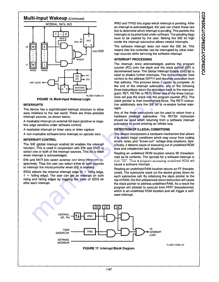
M u lti-In p u t W a k e u p  

(Continued)

INTERNAL  DATA  BUS

TL/DD/11208-21

FIGURE 16. Multi-Input Wakeup Logic


INTERRUPTS

The  device  has  a  sophisticated  interrupt  structure  to  allow 
easy  interface  to  the  real  world.  There  are  three  possible 
interrupt sources,  as shown  below.

A maskable interrupt on external GO input (positive or nega­
tive edge sensitive  under software control)

A  maskable interrupt on timer carry or timer capture 

A  non-maskable software/error interrupt on  opcode zero 

INTERRUPTCONTROL

The  GIE  (global  interrupt  enable)  bit  enables  the  interrupt 
function.  This  is  used  in  conjunction  with  ENI  and  ENTI  to 
select one or both  of the interrupt sources.  This bit is reset 
when  interrupt is acknowledged.

ENI  and  ENTI  bits  select  external  and  timer  interrupts  re­
spectively.  Thus the  user can  select  either or both  sources 

to interrupt the  microcontroller when  GIE is enabled.

IEDG  selects the  external  interrupt  edge  (0  =  rising  edge, 
1  =  falling  edge).  The  user  can  get  an  interrupt  on  both 

rising  and  falling  edges  by  toggling  the  state  of  IEDG  bit 
after each  interrupt.

IPND and TPND bits signal which interrupt is  pending. After 
an interrupt is acknowledged, the user can check these two 
bits to determine which interrupt is pending. This permits the 
interrupts to be prioritized under software. The pending flags 
have  to  be  cleared  by  the  user.  Setting  the  GIE  bit  high 
inside the interrupt subroutine allows  nested  interrupts.

The  software  interrupt  does  not  reset  the  GIE  bit.  This 

means that the controller can  be  interrupted  by other inter­
rupt sources while servicing the software interrupt.

INTERRUPT PROCESSING

The  interrupt,  once  acknowledged,  pushes  the  program 
counter  (PC)  onto  the  stack  and  the  stack  pointer  (SP)  is 
decremented twice. The Global  Interrupt Enable (GIE) bit is 
reset to  disable  further  interrupts.  The  microcontroller then 
vectors to the address 00FFH and resumes execution from 
that  address.  This  process  takes  7  cycles  to  complete.  At 
the  end  of  the  interrupt  subroutine,  any  of  the  following 
three instructions return the processor back to the main pro­
gram: RET,  RETSK or RETI.  Either one of the three instruc­
tions will  pop the  stack into the program counter  (PC).  The 
stack  pointer  is  then  incremented  twice.  The  RETI  instruc­
tion  additionally  sets  the  GIE  bit  to  re-enable  further  inter­
rupts.

Any  of the  three  instructions  can  be  used to  return  from  a 
hardware  interrupt  subroutine.  The  RETSK  instruction 
should  be  used  when  returning  from  a  software  interrupt 
subroutine to  avoid entering  an  infinite  loop.

DETECTION OF ILLEGAL CONDITIONS

The device incorporates a hardware mechanism that allows 

it to  detect  illegal  conditions which  may occur from  coding 
errors,  noise, and “ brown out” voltage drop situations. Spe­
cifically, it detects cases of executing out of undefined ROM 
area and  unbalanced tack  situations.

Reading  an  undefined  ROM  location  returns  00  (hexadeci­
mal)  as its contents. The opcode for a software  interrupt is 
also  “ CO” .  Thus  a  program  accessing  undefined  RGivi  wiii 
cause a software interrupt.

Reading an undefined RAM location returns an FF (hexade­

cimal).  The  subroutine  stack  on  the device grows down  for 
each  subroutine  call.  By initializing  the  stack  pointer to the 
top of RAM, the first unbalanced return instruction will cause 
the stack pointer to address undefined RAM. As a result the 
program  will  attempt  to  execute  from  FFFF  (hexadecimal), 
which  is an  undefined  ROM  location  and will  trigger a soft­
ware  interrupt.

TO
INTERRUPT
LOGIC

FIGURE 17. Interrupt Block Diagram

TL/DD/11208-27

1-67

COP8

20C

J/CO

P8
22C

J/CO

P82

3CJ

Summary of Contents for COP820CJ

Page 1: ...perating at a 1 jus per in struction rate Features Low cost 8 bit Microcontroller n Fully static CMOS n 1 jus instruction time Low current drain Low current static HALT mode Single supply operation 2 5V to 6 0V 1024 x 8 on chip ROM 64 bytes on chip RAM WATCHDOG Timer Comparator Modulator Timer High speed PWM Timer for IR Transmission Multi Input Wakeup on the 8 bit Port L Brown Out Protection 4 hi...

Page 2: ...5 mA CKI 4 MHz Vcc 4 0V tc 2 5 fis 2 0 mA CKI 1 MHz Vcc 4 0V tc 10 jxs 1 5 mA HALT Current with Brown Out Disbled Note 3 VCc 6V CKI 0 MHz 1 10 p A HALT Current with Brown Out Enabled VCc 6V CKI 0 MHz 50 110 juA BrownOut Trip Level 1 8 3 1 4 2 Brown Out Enabled INPUT LEVELS V H V l Reset CKI Logic High 0 8 VCC V Logic Low All Other Inputs 0 2 VCC V Logic High 0 7 VCC V Logic Low 0 2 VCC V Hi Z Inpu...

Page 3: ...low Vcc The effective resistance to Vcc is 750ft typical These two pins will not latch up The voltage at the pins must be limited to less than 14V AC Electrical Characteristics 40 C Ta 85 C unless otherwise specified Parameter Conditions Min Typ Max Units Instruction Cycle Time tc Crystal Resonator 4 5V Vcc 6 0V 1 DC JUS 2 5V VCc 4 5V 2 5 DC JUS R C Oscillator 4 5V VCc 6 0V 3 DC JUS 2 5V VCc 4 5V ...

Page 4: ...5 S K 2 27 G2 G 6 S I 3 26 G1 G 7 C K 0 4 25 G 0 IN T C K I 5 24 RESET w c r snrv CC wnw I0 7 22 D3 1 1 8 21 02 I 2 9 20 01 I 3 10 19 D O L0 C M P 0U T 11 18 L7 M0D0UT L1 CMPIN 12 17 L6 L2 CMPIN 13 16 L5 L3 14 15 L4 T L D D 11208 3 Top View Order Number COPCJ820 XXX N or COPCJ820 XXX WM G4 S0 1 20 G3 TI0 G 5 S K 2 19 G2 G6 SI 3 18 G1 07 C K0 4 17 C O IM T CKI 5 16 RESET vc c 6 15 GND L0 CMP0UT 7 1...

Page 5: ...COP820CJ COP822CJ COP823CJ 1 54 ...

Page 6: ... MIWU high sink current capability L6 MIWU high sink current capability L7 MIWU or MODOUT high sink current capability The selection of alternate Port L functions is done through registers WKEN 00C9 to enable MIWU and CNTRL2 OOCC to enable comparator and modulator All eight L pins have Schmitt Triggers on their inputs PORT G is an 8 bit port with 6 I O pins G0 G5 and 2 input pins G6 G7 All eight G...

Page 7: ...emory is addressed directly by the in struction or indirectly through B X and SP registers The device has 64 bytes of RAM Sixteen bytes of RAM are mapped as registers these can be loaded immediately decremented and tested Three specific registers X B and SP are mapped into this space the other registers are avail able for general usage Any bit of data memory can be directly set reset or tested All...

Page 8: ...a 256tc delay This delay allows the oscillator to stabilize before the device ex its the reset state The delay is not used if the clock option is either R C or external clock The contents of data registers and RAM are unknown following a Brown Out reset The external reset takes priority over Brown Out Reset and will deactivate the 256 tc cycles delay if in progress The Brown Out reset takes priori...

Page 9: ...ke a R C oscillator CKO is available as a general purpose input and or HALT control Table II shows variation in the oscilla tor frequencies as functions of the component R and C values Functional Description Continued TABLE I Crystal Oscillator Configuration R1 R2 C1 C2 CKI Freq Conditions kn Mft PF PF MHz 0 1 30 30 36 10 Vcc 5V 0 1 30 30 36 4 VCC 5V 5 6 1 100 100 156 0 455 in II o o TABLE II RC O...

Page 10: ... and freuqency stability The WATCHDOG timer consisting of an 8 bit prescaler followed by an 8 bit counter is used to gen erate a fixed delay of 256tc to ensure that the oscillator has indeed stabilized before allowing instruction execution In this case upon detecting a valid WAKEUP signal only the oscillator circuitry is enabled The WATCHDOG Counter and Prescaler are each loaded with a value of FF...

Page 11: ...here tc is the instruction cycle time MICROWIRE PLUS OPERATION Setting the BUSY bit in the PSW register causes the MI CROWIRE PLUS arrangement to start shifting the data It gets reset when eight data bits have been shifted The user may reset the BUSY bit by software to allow less than 8 bits to shift The device may enter the MICROWIRE PLUS mode either as a Master or as a Slave Figure 7 shows how t...

Page 12: ...tive edge Upon underflow the contents of the register R1 are automatically copied into the counter The underflow can also be programmed to generate an interrupt Figure 9 T im er C o u n ter The device has a powerful 16 bit timer with an associated 16 bit register enabling it to perform extensive timer func tions The timer T1 and its register R1 are each organized as two 8 bit read write registers ...

Page 13: ...ms The WATCHDOG can be en abled or disabled only once after the device is reset as a result of brown out reset or external reset On power up the WATCHDOG is disabled The WATCHDOG is enabled by writing a 1 to WDREN bit resides in WDREG register Once enabled the user program should write periodically into the 8 bit counter before the counter underflows The 8 bit counter WDCNT is memory mapped at add...

Page 14: ...he HALT mode It is a read only bit WDREN bit resides in a separate register bit 0 of WDREG This bit enables the WATCHDOG timer to generate a reset The bit is cleared upon Brown Out reset or external reset The bit under software control can be written to only once once written to the hardware does not allow the bit to be changed during program execution WDREN 1 WATCHDOG reset is enabled WDREN 0 WAT...

Page 15: ... Timer In this mode an 8 bit register is used to serve as an autoreload register MODRL a 50 Duty Cycle When MC1 is 1 and MC2 MC3 are 0 a 50 duty cycle free running signal is generated on the L7 output pin Figure 14 The L7 pin must be configured as an output pin In this mode the 8 bit counter is clocked by tC Setting the MC1 control bit by software loads the counter with the value of the autoreload...

Page 16: ... REGISTER r 4 INTERNAL DATA BUS k i k 7 6 5 f 0 AUTO RELOAD MC3 MC2 MC1 8 BIT 0 1 R Q S I ILK 8 BIT START STOP 1 IIDERTLCV CNTRL2 REGISTER TIMER Tt UNDERFLOW L7 PIN T L D D 11208 19 UNDERFLOW I I UNDERFLOW u 256 MAX CONTROLLED BY T1 FIGURE 15 Mode 2b Variable Duty Cycle Output T L D D 11208 20 1 65 COP820CJ COP822CJ COP823CJ ...

Page 17: ...rify this procedure Suppose we wish to change the edge select from positive low going high to negative high going low for L port bit 5 where bit 5 has previously been enabled for an input The program would be as follows RBIT 5 WKEN SBIT 5 WKEDG RBIT 5 WKPND SBIT 5 WKEN If the L port bits have been used as outputs and then changed to inputs with Multi Input Wakeup a safety proce dure should also be...

Page 18: ... onto the stack and the stack pointer SP is decremented twice The Global Interrupt Enable GIE bit is reset to disable further interrupts The microcontroller then vectors to the address 00FFH and resumes execution from that address This process takes 7 cycles to complete At the end of the interrupt subroutine any of the following three instructions return the processor back to the main pro gram RET...

Page 19: ...Y ENI GIE The Half Carry bit is also effected by all the instructions that effect the Carry flag The flag values depend upon the in struction For example after executing the ADC instruction the values of the Carry and the Half Carry flag depend upon the operands involved However instructions like SET C and RESET C will set and clear both the carry flags Table XIII lists the instructions that effec...

Page 20: ...the B or X pointer This is a register indirect mode that automati cally post increments or post decrements the B or X pointer after executing the instruction DIRECT The instruction contains an 8 bit address field that directly points to the data memory for the operand IMMEDIATE The instruction contains an 8 bit immediate field as the op erand SHORT IMMEDIATE This addressing mode issued with the LD...

Page 21: ...Set bit 1 to bit Mem bit 0 to 7 immediate RBIT Reset bit 0 to bit Mem IFBIT If bit If bit Mem is true do next instr X Exchange A with memory A Mem LD A Load A with memory A 4 Meml LD mem Load Direct memory Immed Mem 4 Imm LDReg Load Register memory Immed Reg Imm X Exchange A with memory B A B B B 1 X Exchange A with memory X A X X X 1 LD A Load A with memory B A B B B 1 LD A Load A with memory X A...

Page 22: ...1 71 COP820CJ COP822CJ COP823CJ ...

Page 23: ...1 3 4 2 2 OR 1 1 3 4 2 2 XOR 1 1 3 4 2 2 IFEQ 1 1 3 4 2 2 IFGT 1 1 3 4 2 2 IFBNE 1 1 DRSZ 1 3 SBIT 1 1 3 4 RBIT 1 1 3 4 IFBIT 1 1 3 4 Memory Transfer Instructions Bytes Cycles Register Indirect B X Direct Immed Register Indirect Auto Incr Deer B B X X XA 1 1 1 3 2 3 1 2 1 3 LD A 1 1 1 3 2 3 2 2 1 2 1 3 LD B lmm 1 1 LD B lmm 2 3 LD Mem lmm 3 3 2 2 LD Reg lmm 2 3 Memory location addressed by B or X ...

Page 24: ...direct address opcode value opcode class or im mediate operand Complex breakpoints can be ANDed and ORed together Trace information consists of address bus values opcodes and user selectable probe clips status ex ternal event lines The trace buffer can be viewed as raw hex or as disassembled instructions The probe clip bit val ues can be displayed in binary hex or digital waveform for mats During ...

Page 25: ...dering Information Assembler Ordering Information Part Number Package Voltage Range Emulates MH 820CJ20D5PC 20 DIP 4 5V 5 5V COP822CJ MHW 820CJ20DWPC 20 DIP 2 3V 6 0V COP822CJ MHW 820CJ28D5PC 28 DIP 4 5V 5 5V COP820CJ MHW 820CJ28DWPC 28 DIP 2 3V 6 0V COP820CJ Part Number Description Manual COP8 DEV IBMA COP8 Assembler Linker Librarian for IBM PC XT AT or compatible 424410632 001 MACRO CROSS ASSEMB...

Page 26: ... by the Microcontroller Applications Group The Dial A Helper is an Electronic Bul letin Board information system INFORMATION SYSTEM The Dial A Helper system provides access to an automated information storage and retrieval system that may be ac cessed over standard dial up telephone lines 24 hours a day The system capabilities include a MESSAGE SECTION electronic mail for communications to and fro...

Reviews: