7
8
|
ni.com
|
NI 9144 User Guide and Specifications
Table 82.
NI 9236 Scan List Format
Bits
Field
Description
15..10
Clock Divisor
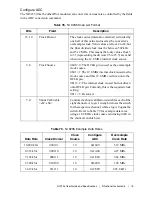
The clock source (internal or external) is divided by
one half of this value and used as the converter’s
oversample clock. Valid values are from 2 to 63, but
the final divided clock must be between 502 kHz and
5.12 MHz. This means that only values from 5 to 51
(representing the divisors 2.5 to 25.5) are valid when
using the 12.8 MHz internal clock source.
9..8
Clock Source
0b00 = 0: The OCLK pin is used as the oversample
clock source.
0b01 = 1: The 12.8 MHz internal clock is used as the
clock source and this 12.8 MHz is driven onto the
OCLK pin.
0b10 = 2: The internal clock is used but not driven
onto OCLK pin. Currently, this is the required clock
setting.
0b11 = 3: Reserved.
7..0
Shunt Cal Enable
<ch7..ch0>
Controls the shunt calibration switch for each of the
eight channels. A logic 1 in any bit closes the switch
for the respective channel, while a logic 0 opens the
switch.
Table 83.
NI 9236 Example Data Rates
Data Rate
Clock Divisor
Clock
Source
Configure
ADC
Oversample
Clock Rate
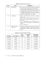
10.000 kS/s
000101
10
0x1600
5.12 MHz
8.333 kS/s
000110
10
0x1A00
4.27 MHz
7.143 kS/s
000111
10
0x1E00
3.66 MHz
2.500 kS/s
010100
10
0x5200
1.28 MHz
1.613 kS/s
011111
10
0x7E00
825.8 kHz
1.250 kS/s
101000
10
0xA200
640.0 kHz
0.980 kS/s
110011
10
0xCE00
502.0 kHz


