background image

NI 9144 User Guide and Specifications

|

© National Instruments

|

25

Refer to the 

C Series Modules with No Configurable Options

 section for all other supported 

C Series modules.

NI 9201/9221

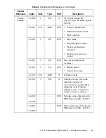
The vendor configuration extensions for the NI 9201/9221 are listed in Table 4.

NI 9201/9221 Scan List

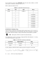
The scan list channel codes consist of two bit fields in a 32-bit entry.

Bits <23..16> describe the data offset to store a conversion at time 

t

, and bits <7..0> describe the 

conversion control code that takes effect two conversions in the future, at time 

t+2

. On the 

NI 9201/9221, this conversion code is a bit flag where bit 0 represents a conversion 
on channel 0, through bit 7 for channel 7.

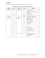
Table 4.  

NI 9201/9221 Vendor Configuration Extensions

Index

Sub

Type

R/W

Description

0x2001

0

ARR:U32

Scan List = 9

1

R

Channels to Convert = <1..8>, default = 8

2..9

R/W

Channel Code

0x2002

0

U32

R/W

Fast Convert = 0/1, default = 1 (fast)

0x2100

0

ARR:U32

Calibration = 32

1

R

Ch0 Offset

2

R

Ch0 Gain

15

R

Ch7 Offset

16

R

Ch7 Gain

17

R

External Calibration, Ch0 Offset

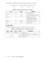
Table 5.  

NI 9201/9221 Scan List Format

Bits

Field

31..24

= 0

23..16

Data Offset[

t

]

15..8

= 0

7..0

Convert Flag[

t

+2]

Summary of Contents for NI 9144

Page 1: ...to a network how to use the NI 9144 chassis features and contains the NI 9144 chassis specifications The NI 9144 is a slave device and requires a compliant EtherCAT Master and network to function Figu...

Page 2: ...ations 15 Safety and Hazardous Locations Standards 16 Appendix 21 Vendor Extensions to the Object Dictionary 21 Supported C Series Modules 24 C Series Modules with No Configurable Options 90 Worldwide...

Page 3: ...ested and complies with the regulatory requirements and limits for electromagnetic compatibility EMC stated in the product specifications These requirements and limits provide reasonable protection ag...

Page 4: ...performance is attained Mounting the NI 9144 Chassis You can mount the chassis in any orientation on a 35 mm DIN rail or on a panel Use the DIN rail mounting method if you already have a DIN rail conf...

Page 5: ...structions record the serial number from the back of the chassis After the chassis is mounted you will not be able to read the serial number Caution Remove any C Series I O modules from the chassis be...

Page 6: ...crews because they are the correct depth and thread for the panel Figure 5 Installing the Panel Mount Accessory on the NI 9144 Chassis Figure 6 Dimensions of NI 9144 Chassis with Panel Mount Accessory...

Page 7: ...s from the DIN rail Use the NI 9915 DIN rail mount kit if you want to mount the chassis on a DIN rail You need one clip for mounting the chassis on a standard 35 mm DIN rail Complete the following ste...

Page 8: ...your LabVIEW target establish a connection with the NI 9144 chassis connect the secondary port of the LabVIEW Real Time target to the NI 9144 IN port Use a standard Category 5 CAT 5 or better Etherne...

Page 9: ...indicates that the power supply connected to the chassis is adequate FPGA LED Open FPGA Mode Only You can program this LED using LabVIEW FPGA RUN and ERR LEDs The RUN LED is green and indicates that t...

Page 10: ...dog Timeout Slave did not receive a scheduled EtherCAT telegram On Operational Inputs and outputs are functional PDI Process Data Interface Watchdog Timeout Slave failed to transfer I O data in schedu...

Page 11: ...erCAT distributed clock DC through DC synchronized mode In free run mode the NI 9144 by default runs its conversion cycle as quickly as the slowest module allows It is possible to slow the free run co...

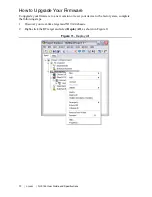
Page 12: ...Firmware To upgrade your firmware to a new version or reset your device to the factory state complete the following steps 1 Discover your real time target and NI 9144 chassis 2 Right click the RT targ...

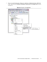
Page 13: ...ional Instruments 13 3 After a successful deployment change the controller to Configuration Mode Right click the RT target and select Utilities Scan Engine Mode Switch to Configuration as shown in Fig...

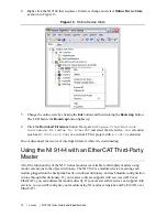
Page 14: ...GA project with a lvbitx extension Do not disconnect the device or interrupt firmware while it is downloading Using the NI 9144 with an EtherCAT Third Party Master All of the functionality of the NI C...

Page 15: ...tion refer to your C Series module documentation Using CoE SDO The CoE protocol does not have a destination port or address so the NI 9144 provides an object dictionary entry that allows addressing su...

Page 16: ...ou need to clean the controller wipe it with a dry towel Screw terminal wiring Gauge 0 20 mm2 24 AWG to 2 1 mm2 14 AWG copper conductor wire with 5 mm 0 20 in to 6 mm 0 24 in of insulation stripped fr...

Page 17: ...by regulated low voltage sources and electronics Caution Do not connect the system to signals or use for measurements within Measurement Categories II III or IV Hazardous Locations U S UL Class I Div...

Page 18: ...27 30 g 11 ms half sine 50 g 3 ms half sine 18 shocks at 6 orientations Operating vibration random IEC 60068 2 64 5 grms 10 to 500 Hz Operating vibration sinusoidal IEC 60068 2 6 5 g 10 to 500 Hz Cabl...

Page 19: ...and laboratory use EN 61326 1 IEC 61326 1 Class A emissions Basic immunity EN 55011 CISPR 11 Group 1 Class A emissions AS NZS CISPR 11 Group 1 Class A emissions FCC 47 CFR Part 15B Class A emissions...

Page 20: ...nmentally responsible manner NI recognizes that eliminating certain hazardous substances from our products is beneficial to the environment and to NI customers For additional environmental information...

Page 21: ...Series modules have vendor extensions to the standard These extensions are described here Note Most object dictionary entries are set to usable defaults during the NI 9144 s transition from INIT to PR...

Page 22: ...t to 0 to operate at the minimum cycle Set to 1 000 000 for a 1 mS cycle 1 kHz 2 R W Disables multiple scans Setting the field to 1 disables multiple scan ability Even when a module has enough time du...

Page 23: ...3 0 U32 R W Error acknowledgement or status 0x2005 0 U8 R W Refresh period Conversion format 0x2100 0 N ARR R Calibration data 0x3002 0 U32 R Number of scans This index reports the number of conversio...

Page 24: ...g supported C Series modules NI 9201 9221 NI 9203 NI 9205 9206 NI 9207 NI 9208 NI 9211 NI 9212 NI 9213 NI 9214 NI 9215 NI 9217 NI 9218 NI 9219 NI 9220 NI 9222 9223 NI 9225 NI 9227 NI 9229 9239 NI 9233...

Page 25: ...n control code that takes effect two conversions in the future at time t 2 On the NI 9201 9221 this conversion code is a bit flag where bit 0 represents a conversion on channel 0 through bit 7 for cha...

Page 26: ...d when the inputs are grounded Note LSB weight is referred to as Gain in the object dictionary The calibration data is stored in a U32 array though each Offset field subindex 1 3 5 and so on should be...

Page 27: ...dor Configuration Extensions Index Sub Type R W Value 0x2001 0 ARR U32 Scan List 9 1 R Channels to Convert 1 8 default 8 2 9 R W Channel Code 0x2002 0 U32 R W Unipolar Channel Mask 0x2100 0 ARR U32 Ca...

Page 28: ...the result is bipolar signed or unipolar unsigned and bits 2 0 are the channel number reversed For example the scan list entry 0x00010006 indicates that this scan gets stored at address 1 and the con...

Page 29: ...in offset from channel to channel is negligible The calibration data gives one offset and eight gains for each mode a total of 2 offsets and 16 gains in total All channels in a given mode use the sam...

Page 30: ...Definition Icorrected pA Calibrated current Iraw bits The raw code from the NI 9203 Iexpected0mA bits Expected code at 0 mA 0 bits for 0 20 mA range 32768 bits for 20 mA range LSBweight pA bit Number...

Page 31: ...bit entry 0x2100 0 ARR U32 Calibration 24 1 R Coeff 3 2 R Coeff 2 3 R Coeff 1 4 R Coeff 0 5 R 10 V offset 6 R 10 V gain 7 R 5 V offset 13 R User calibration Coeff 3 Table 15 Scan List Format Bits Fiel...

Page 32: ...ions in the future at time t 2 On the NI 9205 9206 this conversion code is listed in Table 16 Table 16 NI 9205 9206 Conversion Code Bits Field 15 13 001 Read AI 12 11 Bank 01 Channels 0 15 10 Channels...

Page 33: ...tion formula 2 Select the 32 bit gain value for a particular range 3 Select the 32 bit offset value to be interpreted as a signed int for a particular range Table 17 NI 9205 9206 Scan List Format Inde...

Page 34: ...For more information refer to the NI 9201 9221 section of this guide Note The offset and gain values of the NI 9205 9206 are different from those of the NI 9201 9221 Use 10E 9 for the offset value and...

Page 35: ...ration tables NI 9208 The vendor configuration extensions for the NI 9208 are listed in Table 21 Table 19 NI 9207 Conversion Speed Control Speed Control Meaning Conversion Rate 0 High Accuracy 62 5 ms...

Page 36: ...NI 9208 has sixteen total channels that can be measured NI 9208 Calibration Data Calibration data is set up by driver during initialization and the calibration conversion is performed on the module A...

Page 37: ...n channel always measured in a 2 5 V range 5 one auto zero channel always measured in a 80 mV range Table 25 contains the default scan list NI 9211 Calibration Data Calibration data is set up by the d...

Page 38: ...defined as listed in Table 28 Table 26 NI 9212 Vendor Configuration Extensions Index Sub Type R W Description 0x2002 U32 R W Channel Speed Control 2 8 9 or 15 default 15 0x2003 ARR U32 R Open Thermoc...

Page 39: ...resents raw TC voltage BitTC represents binary bits for the TC After calculating the CJC and the TC voltage use the NI 9212 Getting Started lvproj located by default in the LabVIEW examples CompactRIO...

Page 40: ...asured 0 15 sixteen thermocouple channels always measured in a 78 125 mV range 16 one cold junction channel always measured in a 2 5 V range 17 one auto zero channel always measured in a 78 125 mV ran...

Page 41: ...to calculate raw voltage for the cold junction compensation CJC where VCJCvoltage represents raw CJC voltage BitCJC represents binary bits for the CJC Use the following equation to calculate raw volt...

Page 42: ...set represents the offset constant The value is 1 The constant is the typical temperature gradient between the CJC sensor and the TC cold junction NI 9214 The vendor configuration extensions for the N...

Page 43: ...easured in a 78 125 mV range 16 One auto zero channel always measured in a 78 125 mV range 17 Cold junction channel 0 always measured in a 2 5 V range 18 Cold junction channel 1 always measured in a 2...

Page 44: ...raw CJC voltage BitCJC represents binary bits for the CJC Use the following equation to calculate raw voltage for the thermocouple TC where VTCvoltage represents raw TC voltage BitTC represents binary...

Page 45: ...ain in the object dictionary The NI 9215 EEPROM stores these two constants for each channel The host can then take these constants and adjust the raw data into calibrated data The calibration data is...

Page 46: ...iguration extensions for the NI 9217 are listed in Table 41 Table 41 NI 9217 Vendor Configuration Extensions Index Sub Type R W Description 0x2001 0 ARR U32 Scan List 5 1 R Channels to Convert 1 4 def...

Page 47: ...time t 2 The conversion code is listed in Table 44 Note The conversion rate for every channel must match the value of the conversion speed control in 0x2002 For example the scan list entry 0x00000001...

Page 48: ...umber of ohms per bit measured when the inputs are grounded Note LSB weight is referred to as Gain in the object dictionary The calibration data is stored in a U32 array though each Offset field subin...

Page 49: ...de for all channels by default Table 47 NI 9218 Vendor Configuration Extensions Index Sub Type R W Description 0x2002 0 U32 R W Configure Module default 0x00010106 0x2100 0 ARR U32 Calibration 48 1 R...

Page 50: ...mode calibration information for the channel 15 14 Reserved 13 Offset Cal Enable ch0 Controls the offset calibration mode Offset calibration mode disconnects both signal input pins and forces the cha...

Page 51: ...49 NI 9218 Modes Mode Index 16 V 1 5 V 2 16 V with Power Sensor 3 60 V 4 65 mV 5 65 mV with Power Sensor 6 20 mA 7 20 mA with Power Sensor 8 22 mV V Bridge 2 V Ex 9 22 mV V Bridge 3 3 V Ex 10 Table 50...

Page 52: ...ollowing equation to generate corrected data where y represents the calibrated data for the voltage current or bridge m represents the ADC data x represents raw data for the voltage current or bridge...

Page 53: ...dex Sub Type R W Description 0x2001 0 ARR U32 Command List 33 1 R Command Count 1 32 default 32 2 33 R W Configuration Command 0x2002 1 ARR U32 R Error Status 0x2005 0 U32 R W ADC Format 0x2100 0 ARR...

Page 54: ...nel over current condition occurs on any of the channels of the NI 9219 such as configure channels in 4 wire resistance mode and do not connect a resistor to the channel the firmware sets a bit in the...

Page 55: ...d in Table 54 Table 54 NI 9219 Channel Calibration Entry Number Mode Range 1 Voltage 60 V 2 15 V 3 4 V 4 1 V 5 125 mV 6 Current 25 mA 7 4 Wire Resistance 10 k 8 1 k 9 2 Wire Resistance 10 k 10 1 k 11...

Page 56: ...19 Eight configuration commands must be sent for each of the four channels This is true even if you are only using a subset of the four channels Each of the eight configuration commands is 1 Byte each...

Page 57: ...nfigData 0 shiftBool 0x01 crcShiftReg 0 crcShiftReg 2 if dataBool shiftBool crcShiftReg 0x8C crcShiftReg crcShiftReg 1 return crcShiftReg NI 9219 Configuration Command Whether you are using the channe...

Page 58: ...0 3 5 0 4 0 Configuration Type Configuration Type values Conversion Time Mode Range Calibration Offset 2 LSB Calibration Offset 1 Calibration Offset 0 MSB Calibration Gain 2 LSB Calibration Gain 1 Ca...

Page 59: ...ge 0x00 Voltage 60 V 0x01 15 V 0x02 3 75 V 0x03 1 V 0x04 125 V 0x05 Current 25 mA 0x06 Resistance 10K 4w 0x07 1K 4w 0x08 10K 2w 0x09 1K 2w 0x0A TC TC 0x0B RTD Pt1000 4w 0x0C Pt100 4w 0x0D Pt1000 3w 0x...

Page 60: ...ption 0x01 Mode and Range Configuration Byte Channel 0 0x01 Data Byte 0x46 CRC value 0x1F Conversion Time Channel 0 0x01 Data Byte 0xC6 CRC value 0x04 Calibration Offset MSB Channel 0 0x7F Data Byte 0...

Page 61: ...6 CRC value 0x45 Calibration Offset Byte 2 Channel 1 0xFF Data Byte 0x94 CRC value 0x46 Calibration Offset LSB Channel 1 0x86 Data Byte 0xE0 CRC value 0x48 Calibration Gain MSB Channel 1 0x6C Data Byt...

Page 62: ...value 0x86 Calibration Offset LSB Channel 2 0xC8 Data Byte 0xC2 CRC value 0x88 Calibration Gain MSB Channel 2 0x6C Data Byte 0x96 CRC value 0x89 Calibration Gain Byte 2 Channel 2 0xB0 Data Byte 0xF4 C...

Page 63: ...nnel 3 0xFF Data Byte 0x1C CRC value 0xC6 Calibration Offset LSB Channel 3 0xD3 Data Byte 0xCA CRC value 0xC8 Calibration Gain MSB Channel 3 0x6C Data Byte 0xB4 CRC value 0xC9 Calibration Gain Byte 2...

Page 64: ...t the raw data into calibrated data The calibration data is stored in a U32 array though each Offset field subindex 1 3 5 and so on should be interpreted as a signed value Use the calibration coeffici...

Page 65: ...tants and adjust the raw data into calibrated data The calibration data is stored in a U32 array though each Offset field subindex 1 3 5 and so on should be interpreted as a signed value Use the calib...

Page 66: ...ize to other modules and free runs at its own fixed rate For more information refer to the NI 9233 Configure ADC section of this user guide Table 65 NI 9225 Vendor Configuration Extensions Index Sub T...

Page 67: ...ynchronize to other modules and free runs at its own fixed rate For more information refer to the NI 9233 Configure ADC section of this user guide Table 66 NI 9227 Vendor Configuration Extensions Inde...

Page 68: ...channel has an associated LSB weight which is the number of volts per bit and an offset which is the number of volts per bit measured when the inputs are grounded Note LSB weight is referred to as Ga...

Page 69: ...dules and free runs at its own fixed rate The vendor configuration extensions for the NI 9233 are listed in Table 69 NI 9233 Configure ADC The NI 9233 and NI 9229 9239 converts at various rates contro...

Page 70: ...2 8 MHz internal clock source 1 0 Clock Source 2 0b00 0 The OCLK pin is used as the oversample clock source 0b01 1 The 12 8 MHz internal clock is used as the clock source and this 12 8 MHz is driven o...

Page 71: ...ht is referred to as Gain in the object dictionary The calibration data is stored in a U32 array though each Offset field subindex 1 3 5 and so on should be interpreted as a signed value Use the calib...

Page 72: ...E operations switches the AC DC relay to AC mode and enables the IEPE relay to send the current to the IEPE sensor 12 Ch2 AC DC AC DC 2 Controls the AC DC relay when IEPE is not selected If IEPE is en...

Page 73: ...ual to 1 256 times this oversample clock frequency Valid values for Clock Divisor are from 1 to 31 and the final divided clock must be between 100 KHz and 12 8 MHz 1 0 Clock Source 0b00 0 The OCLK pin...

Page 74: ...tion extensions for the NI 9235 are listed in Table 77 The NI 9235 is a DSA module and as such does not synchronize with other modules but free runs at its own fixed rate Table 76 NI 9234 Scan List Fo...

Page 75: ...as the oversample clock source 0b01 1 The 12 8 MHz internal clock is used as the clock source and this 12 8 MHz is driven onto the OCLK pin 0b10 2 The internal clock is used but not driven onto OCLK p...

Page 76: ...and the excitation voltage termed Vr However typical quarter bridge measurements are denominated in strain which require not only conversion in the strain equation but also the acquisition and use of...

Page 77: ...Table 81 The NI 9236 is a DSA module and as such it does not synchronize with other modules but free runs at its own fixed rate Configure ADC The NI 9236 like the other DSA modules can convert at vari...

Page 78: ...nal clock is used as the clock source and this 12 8 MHz is driven onto the OCLK pin 0b10 2 The internal clock is used but not driven onto OCLK pin Currently this is the required clock setting 0b11 3 R...

Page 79: ...quarter bridge measurements are ultimately denominated in strain which require not only conversion in the strain equation but also the acquisition and use of an unstrained measurement as explained be...

Page 80: ...16 1 R Ch0 Offset 2 R Ch0 Gain 3 R Ch1 Offset 8 R Ch3 Gain 9 R External Ch0 Offset Table 86 NI 9237 Scan List Format Bits Field Description 31 23 Reserved 22 18 Clock Divisor The NI 9237 divides the...

Page 81: ...annel while a logic 0 disables it 7 Reserved 6 4 Excitation Sets the excitation voltage setting All channels share the same excitation voltage 0b000 0 2 5 V The OCLK pin is used as the oversample cloc...

Page 82: ...ugh each Offset field subindex 1 3 5 and so on should be interpreted as a signed value Table 87 NI 9237 Example Data Rates Data Rate Clock Divisor Clock Source Rate Byte Oversample Clock Rate 50 000 k...

Page 83: ...n Table 89 As a DSA module the NI 9242 9244 does not synchronize to other module and free runs at its own fixed rate NI 9242 9244 Configure ADC The NI 9242 9244 converts at various rates controlled by...

Page 84: ...256 times this oversample clock frequency Valid values for Clock Divisor are from 1 to 31 1 0 Clock Source 2 0b00 0 The OCLK pin is used as the oversample clock source 0b01 1 The 12 8 MHz internal cl...

Page 85: ...nts raw data returned by the NI 9242 9244 Vcorrected represents the corrected voltage value NI 9263 The vendor configuration extensions for the NI 9263 are listed in Table 92 NI 9263 Calibration Data...

Page 86: ...tion Data The NI 9264 has 16 channels with a nominal range of 10 5 V Each channel has an associated LSB weight which is the number of volts per bit and an offset which is the number of volts per bit m...

Page 87: ...9265 Error Status Each channel has open loop detection circuitry that reports an error whenever the load is disconnected and the current is set to a value higher than 0 mA On the cycle after the erro...

Page 88: ...e interpreted as a signed value Use the calibration coefficients with the following equation to generate corrected data where Code represents the code returned by the NI 9265 Idesired represents the c...

Page 89: ...calibration data is stored in a U32 array though each Offset field subindex 1 3 5 and so on should be interpreted as a signed value Use the calibration coefficients with the following equation to gene...

Page 90: ...el The host takes the constants and adjusts the raw data in calibrated data The calibration data is stored in a U16 array Use the calibration coefficients with the following equation to generate corre...

Page 91: ...THE ACCURACY OF THE INFORMATION CONTAINED HEREIN AND SHALL NOT BE LIABLE FOR ANY ERRORS U S Government Customers The data contained in this manual was developed at private expense and is subject to th...

Page 92: ...e direction control field has one bit for each I O pin with bit 0 matching channel 0 and so forth 0 in the direction control indicates that I O is an input 1 indicates an output Note Both the input an...

Page 93: ...index 0x2001 Current Limit Select with channel 0 controlled by bits 0 and 1 NI 9478 Direction Control Table 108 NI 9476 Vendor Configuration Extensions Index Sub Type R W Description 0x2002 0 U32 R E...

Page 94: ...field has seven bits to ignore and one bit bit 0 that when set indicates that the module in an over temperature condition Refresh Period This is the period over which output values that may have expe...

Page 95: ...s Visit ni com register to register your National Instruments product Product registration facilitates technical support and ensures that you receive important information updates from NI National Ins...

Reviews: