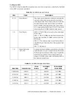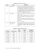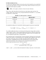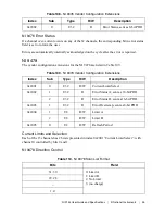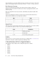
NI 9144 User Guide and Specifications
|
© National Instruments
|
8
1
17..16
Clock Source
—
15..12
Shunt Cal Enable
<ch3..ch0>
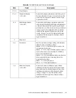
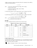
Controls the shunt calibration switch for each of
the four channels. A logic 1 in any bit closes the
switch for the respective channel, while a logic
0 opens the switch.
11..8
Half Bridge Enable
<ch3..ch0>
Controls the half bridge completion option for
each channel. Enabling half bridge completion for
a channel disconnects the negative signal input
pin from the rest of the circuit, and uses an internal
voltage equal to the midpoint of the excitation
voltage as the negative input to the rest of the
circuit. A logic 1 in any bit enables half bridge
completion for the respective channel, while a
logic 0 disables it.
7
Reserved
—
6..4
Excitation
Sets the excitation voltage setting. All channels
share the same excitation voltage.
0b000 = 0: 2.5 V, The OCLK pin is used as the
oversample clock source.
0b001 = 1: 3.3 V, The 12.8 MHz internal clock is
used as the clock source and this 12.8 MHz is
driven onto the OCLK pin.
0b010 = 2: 5.0 V, The internal clock is used but not
driven onto OCLK pin. Currently, this is the
required clock setting.
0b011 = 3: 10.0 V, Reserved.
0b1xx = 4..7: External Excitation.
3..0
Offset Cal Enable
<ch3..ch0>
Controls the offset calibration mode. Offset
calibration mode disconnects both signal input
pins and forces the channel inputs to zero volts,
enabling measurement of the channel’s offset
voltage. A logic 1 in any bit enables offset
calibration for the respective channel, while a
logic 0 disables it.
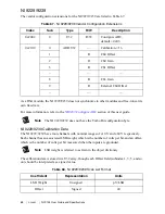
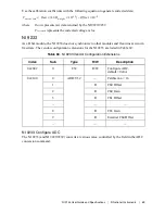
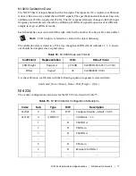
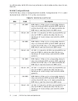
Table 86.
NI 9237 Scan List Format (Continued)
Bits
Field
Description


