IDT Transparent Mode Operation
Generic PCI to PCI Bridge Register Definition
PES12N3 User Manual
9 - 44
June 7, 2006
Notes
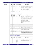
17:13
TSTCLK0SEL
RW
0x0
Test Clock 0 Output Select. This field selects the clock
output driven on the TSTCLK0 pin (GPIO[6] alternate func-
tion).
0x0 - (lane0) Lane 0 recovered clock divided by 40.
1
0x1 - (lane1) Lane 1 recovered clock divided by 40.
0x2 - (lane2) Lane 2 recovered clock divided by 40.
0x3 - (lane3) Lane 3 recovered clock divided by 40.
0x4 - 0x7 Reserved.
0x8 - (lane8) Lane 8 recovered clock divided by 40.
0x9 - (lane9) Lane 9 recovered clock divided by 40.
0xA - (lane10) Lane 10 recovered clock divided by 40.
0xB - (lane11) Lane 11 recovered clock divided by 40.
0xC - 0xF Reserved.
0x10 - (lane16) Lane 16 recovered clock divided by 40.
0x11 - (lane17) Lane 17 recovered clock divided by 40.
0x12 - (lane18) Lane 18 recovered clock divided by 40.
0x13 - (lane19) Lane 19 recovered clock divided by 40.
0x14 - 0x17 Reserved.
0x18 - (serdes0) SerDes 0 250 MHz clock output divided
by four. This SerDes is used to generate the core
clock.
0x19 - Reserved.
0x1A - (serdes2) SerDes 2 250 MHz clock output divided
by four.
0x1B - Reserved.
0x1C - (serdes4) SerDes 4 250 MHz clock output divided
by four.
0x1D - 0x1F Reserved.
22:18
TSTCLK1SEL
RW
0x0
Test Clock 1 Output Select. This field selects the clock
output driven on the TSTCLK1 pin (GPIO[7] alternate func-
tion).
See TSTCLK0SEL (above) for encoding of this field.
24:23
Reserved
RO
0x0
26:25
REFCLKTERM
RW
0x0
PCI Express Reference Clock Termination This field
controls the termination resistor value between the REF-
CLKP[1:0] and REFCLKN[1:0] inputs.
0x0 - (ohms110) 110 ohms.
0x1 - (ohms100) 100 ohms.
0x2 - (ohms96) 96 ohms.
0x3 - (ohms90) 90 ohms.
31:27
Reserved
RO
0x0
1.
Should be 62.5 MHz.
Bit
Field
Field
Name
Type
Default
Value
Description
Summary of Contents for 89HPES12N3
Page 10: ...IDT Table of Contents PES12N3 User Manual iv June 7 2006 Notes...
Page 14: ...IDT List of Figures PES12N3 User Manual viii June 7 2006 Notes...
Page 36: ...IDT Clocking Reset and Initialization Reset PES12N3 User Manual 2 8 June 7 2006 Notes...
Page 40: ...IDT Link Operation Slot Power Limit Support PES12N3 User Manual 3 4 June 7 2006 Notes...
Page 50: ...IDT Switch Operation Switch Core Errors PES12N3 User Manual 4 10 June 7 2006 Notes...
Page 54: ...IDT Power Management Active State Power Management PES12N3 User Manual 5 4 June 7 2006 Notes...
Page 62: ...IDT Hot Plug and Hot Swap Hot Swap PES12N3 User Manual 6 8 June 7 2006 Notes...
Page 78: ...IDT SMBus Interfaces Slave SMBus Interface PES12N3 User Manual 7 16 June 7 2006 Notes...
Page 148: ...IDT Test and Debug SerDes Test Clock PES12N3 User Manual 10 6 June 7 2006...
Page 158: ...IDT JTAG Boundary Scan Usage Considerations PES12N3 User Manual 11 10 June 7 2006 Notes...


