background image

Integrated

Circuit

Systems, Inc.

General Description

Features

ICS1890

10Base-T/100Base-TX Integrated PHYceiver™

ICS1890RevG 10/21/97

Block Diagram

•

One chip integrated physical layer

•

All CMOS, Low power design (<200mA max)

•

Small footprint 64-pin 14mm

  2

 QFP package

•

ISO/IEC 8802-3 CSMA/CD compliant

•

Media Independent Interface (MII)

•

Alternate 100M stream and 10M 7-wire serial

interfaces provided

•

10Base-TX Half & Full Duplex

•

100Base-TX Half & Full Duplex

•

Fully integrated TP-PMD including Stream

Cipher Scrambler, MLT-3 encoder,  Adaptive

Equalization,  and Baseline  Wander Correction

Circuitry

PHYceiver and QuickPoll are  trademarks of Integrated

Circuit Systems, Inc. Patents  pending.
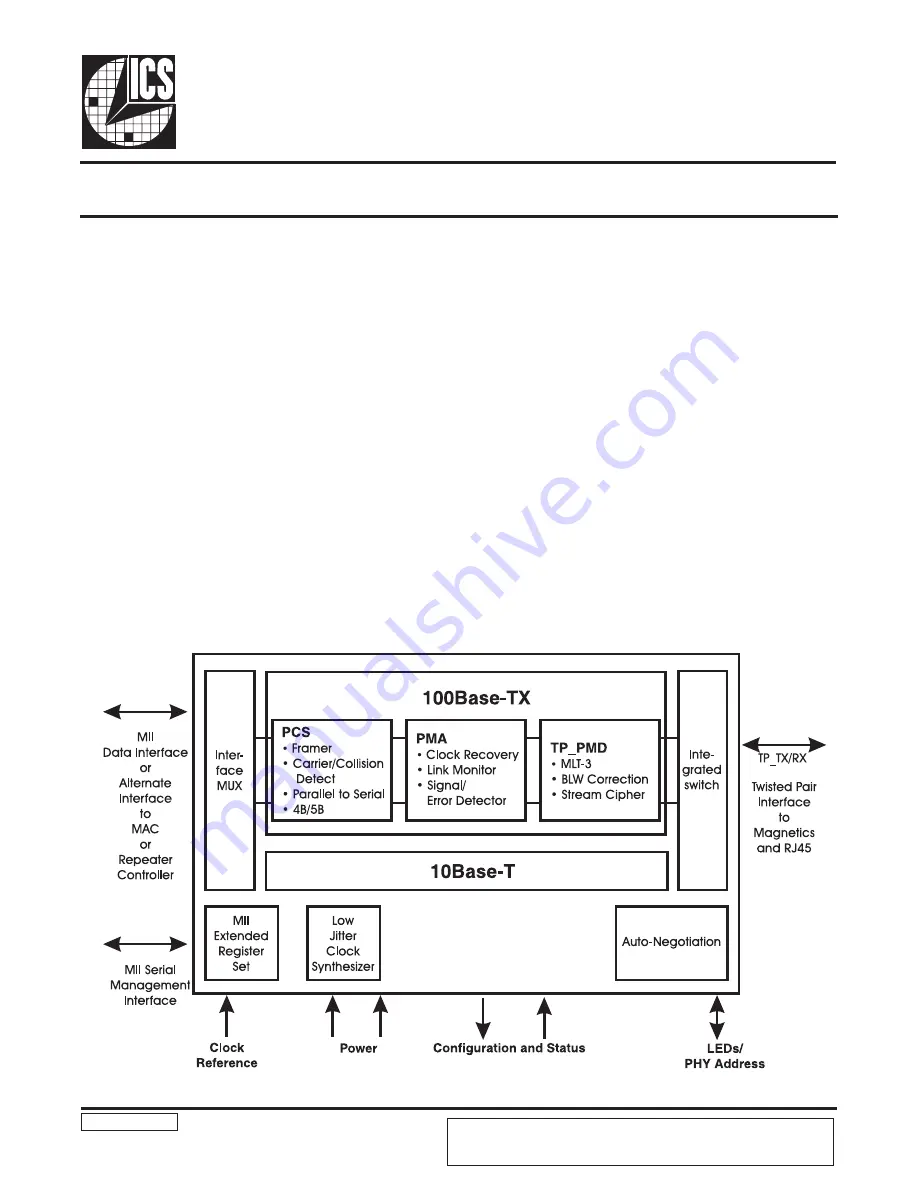
The 

ICS1890 

is a fully integrated physical layer device

supporting 10 and 100Mb/s CSMA/CD Ethernet applications.

DTE (adapter cards or motherboards), switching hub, repeater

and router applications are fully supported. The 

ICS1890

is compliant with the ISO/IEC 8802-3 Ethernet standard

for 10 and 100Mb/s operation. A Media Independent Interface

allowing direct chip-to-chip connection, motherboard-to-

daughterboard connection or connection via an  AUI-like

cable is  provided.  A station management interface is

provided to enable command information and status

information exchange. The 

ICS1890 

interfaces directly to

transmit and receive isolation transformers and can support

shielded twisted pair (STP) and unshielded twisted pair

(UTP) category 5 cables up to 105 meters. Operation in half

duplex or full duplex modes at either 10 or 100 Mbps

speeds is possible with control by  Auto-Negotiation or

manual selection. By employing  Auto-Negotiation the

technology capabilities of the remote link partner may be

determined and operation automatically adjusted to the

highest performance common operating mode.

ICS reserves the right to make changes in the device data identified in this publication

without further notice. ICS advises its customers to obtain the latest version of all

device data to verify that any information being relied upon by the customer is current

and accurate.

Summary of Contents for PHYceiver ICS1890

Page 1: ...IEC 8802 3 Ethernet standard for 10 and 100Mb s operation AMedia Independent Interface allowing direct chip to chip connection motherboard to daughterboard connection or connection via an AUI like cab...

Page 2: ...and detects the idle condition This allows the higher levels to determine the integrity of the connection In the 100Base TX mode a continuous stream of scrambled ones is transmitted signifying the id...

Page 3: ...the Electricals section of the data sheet Auto Negotiation AlinkcanautomaticallybeestablishedusingAuto Negotiation When enabled Auto Negotiation will exchange information about the local node s capab...

Page 4: ...implements a fully compliant IEEE 802 3u Media Independent Interface for connection to MACs or repeaters allowing connection between the ICS1890 and MAC on the same board motherboard daughter board or...

Page 5: ...k rate The Stream Interface provides a CRS signal by continuing to use the logic that is bypassed by this interface This gives a carrierindicationfasterthanispossiblefromtheMAC Repeater since the bits...

Page 6: ...1 RXD3 RXD2 RXD1 RXD0 10RD CRS 10CRS COL 10COL LSTA LSTA 1 Error generation and detection is not supported by 10Base T Other mode configuration pins behave identically regardless of which data interfa...

Page 7: ...ition to the connection of the crystal between these pins a capacitor from REF_IN and REF_OUT to ground is necessary to neutralize the capacitance of the crystal Since these capacitors are nominally i...

Page 8: ...o establish a connection with the remote partner using the highest performance common connection technology The ICS1890 auto negotiation logic is designed to operate with legacy 10Base T networks or n...

Page 9: ...gle bit corresponding to that technology in the AN Link Partner Abilities Register either bit 5 7 or 5 5 and finally indicates Auto Negotiation Complete The entire process in either case usually takes...

Page 10: ...used This coding scheme maps a 4 bit nibble to a 5 bit code group Since this gives 32 possible symbols andthedataonlyrequires16symbols 16symbolsaredesignated control or invalid The control symbols use...

Page 11: ...1 C Data C 1100 11010 D Data D 1101 11011 E Data E 1110 11100 F Data F 1111 11101 V Invalid undefined 00010 V Invalid undefined 00011 V Invalid undefined 00101 V Invalid undefined 00110 V Invalid unde...

Page 12: ...a low jitter reference frequency Signal Detector The ICS1890 Signal Detector is part of the clock recovery PLL It detects a Receive Signal Error if no receive signal is received and detects a PLL Loc...

Page 13: ...cification uses a stream cipher scrambler to minimize peak amplitudes in the frequency spectrum However the nature of the stream cipher and MLT 3 encoding is such that long run lengths of zeroes and o...

Page 14: ...d data The adaptive equalizer picks the best of 32 equalization settings and Fixes this value into theequalizationregister Thissettingprovidesthebestrecovery of the transmitted data with lowest Bit Er...

Page 15: ...Hz clock is synthesized for serial transactions Clock Recovery The PLL synchronizes on the MAC frame preamble and then begins recovering data normally Idle Function The Idle function is used to keep a...

Page 16: ...n to the MH Clock Synthesis A 2 5MHz clock is synthesized for nibble wide transactions A 10MHz clock is synthesized for serial transactions Clock Recovery The PLL synchronizes on the MAC fram preamble...

Page 17: ...ined below Preamble 11 11 32 ones SOF 01 2 bits Op Code 10 read 01 write 2bits Address AAAAA 5 bits Register RRRRR 5 bits TA NN 2 bits Data DD DD 16 bits Idle Zo high impedance Preamble The ICS1890 lo...

Page 18: ...ogic one to this type of bit may prevent the device from operating normally ReadWrite RW bits may be read and may be written to any value Default Values No default value 0 Default to logic zero 1 Defa...

Page 19: ...e collision detection circuitry is also disabled unless the collision test command bit is set Data presented to the MII transmit data path is returned to the MII receive data path The delay from the a...

Page 20: ...ter it has been set to a logic one will cause theICS1890to power up its logic and then reset all error conditions It then enables transmit data and the MII interface Isolate bit 10 Setting this bit to...

Page 21: ...t on ICS1890 operation These bits may however be set using the Command Override mechanism This should only be done in accordance with the IEEE 802 3 standard MF Preamble Suppression bit 6 This bit is...

Page 22: ...otiation Link Status bit 2 When set to a logic one this bit indicates that the Link Monitor has established a valid link If the Link Monitor detects a link failure this bit is set to a logic zero and...

Page 23: ...ntifier bits 3 18 bits 15 0 Thisfieldcontainsthelowest16bitsoftheIEEEOUIexcluding OUI maps to bit 15 of the register OUI Formatting Information The ICS OUI is shown belowwithinformationonmappingtheOUI...

Page 24: ...EEE OUI Bit 19 of the OUI maps to bit 15 of the register Manufacturer s Model Number bits 5 0 bits 9 4 Model Part 1 ICS1889 2 ICS1890 Revision Number bits 3 0 bits 3 0 The revision number will be incr...

Page 25: ...ys returned Bit Definition When bit 0 When bit 1 Access Default Hex 15 Next Page always 0 not capable of sending next pages RO 0 0 14 Reserved by IEEE always 0 RO 0 13 Fault Indication to link partner...

Page 26: ...set to SW these bits are set to the values specified in the MII Status register When the HW SW pin is set to HW and ANSEL is enabled the single bit corresponding to the values of the DPXSEL and 10 100...

Page 27: ...or Field bits 4 0 This 5 bit field indicates the technology supported by the link partner A valid IEEE 802 3 link partner will always signal 00001 Acode of 00010 indicates an IEEE 802 9a partner All o...

Page 28: ...tive link code words have been received from the link partner Link Partner Auto Negotiation Able bit 0 If set to a logic one this bit indicates that the link partner is able to participate in the auto...

Page 29: ...value of these bits is unspecified and may be a logic zero or one NRZ NRZ1 Encoding bit 3 When this bit is 1 normal NRZ1 encoding of data is performed for 100Base TX When this bit is 0 NRZ coding is u...

Page 30: ...nition When bit 0 When bit 1 Access Default Hex 15 Data Rate 10 Mb s negotiated 100 Mb s negotiated RO 14 Duplex half duplex negotiated full duplex negotiated RO 13 Auto Negotiation Progress Monitor b...

Page 31: ...ontents of register 17 Invalid Symbol bit 7 If set to a logic one the invalid symbol indicates that an invalid symbol has been detected in a received frame since the bit was last reset This bit will r...

Page 32: ...The read value of this bit is undefined Auto Polarity Inhibit bit 3 When this bit is set to a logic one correction for reversed receive data wires is disabled When this bit is set to a logic Zero rev...

Page 33: ...en this bit is set to a logic one the 10Base T Link Integrity Test state machine is forced into the Link Pass state regardless of the line conditions This can be useful in debugging a bad link segment...

Page 34: ...L controls the data rate setting When this bit is a logic one software bits have priority over hardware pin settings The 10 100SEL pin becomes an output indicating the link speed when LSTA the link is...

Page 35: ...ts are reserved for ICS use They must only be written as logic zero Writing a logic one to any of these bits may prevent the device from operating normally The value of these bits when read is unspeci...

Page 36: ...Twisted Pair Transmit Data Twisted Pair Receive Data Twisted Pair Receive Data 10M transmit Current Set Resistor 100M Transmit Current Set Resistor NOD REP MII SI 10 LP HW SW 10 100SEL DPXSEL ANSEL IT...

Page 37: ...890 synchronouslywiththeTransmitClockwhenTXENisasserted When TXEN is de asserted theICS1890 is unaffected by the state of TXD1 Transmit Data 0 TXD0 Transmit Data 0 TXD0 is the least significant bit of...

Page 38: ...t False carrier detect is signaled so that repeater applications can preventthepropagationoffalsecarrierdetection RXERalways transitions synchronously with RXCLK The assertion of Receive Error RXER fo...

Page 39: ...ontains the new 100M Stream Interface pseudo pin name followed by the real MII Data Interface pin name that it is mapped onto 100M Stream Interface provides a lower latency parallel interface producin...

Page 40: ...t Clock Receive Clock SRCLK RXCLK The Receive Clock SRCLK is sourced by the ICS1890 TherearetwopossiblesourcesfortheReceiveClock SRCLK When a carrier is present on the receive pair the source is the r...

Page 41: ...Receive Clock 10RCLK is sourced by theICS1890 and is 10 MHz in frequency There are two possible sources for the Receive Clock When a carrier is present on the receive pair the source is the recovered...

Page 42: ...escription also contains the new Link Pulse Interface pseudo pin name followed by the real MII Data Interface pin name that it is mapped onto MII Link Pulse TXCLK LTCLK TXEN TXER LPTX TXD3 TXD2 XD1 TX...

Page 43: ...e value and tolerance of this resistor is specified in the Electricals section 100M Transmit Current Set Resistor 100TCSR A resistor is required to be connected between this pin and the nearest transm...

Page 44: ...ow when Half Duplex is selected and highwhenFullDuplexisselectedwhichgivesthesameindication as register bit 17 14 In Full Duplex mode CRS is asserted only on receive activity In Full Duplex mode COLis...

Page 45: ...of RESET the device will begin to complete its reset cycle Upon comple tion the ICS1890 will be initialized its default state While this pin is held low the device is kept in its low power mode Power...

Page 46: ...e to turn on the LED when either transmit or receive activity is detected This signal is stretched to ensure that a single activity event will be seen If the activity is continuous the LED will appear...

Page 47: ...N C 13 ITCLS I TTL compatible Invert Transmit Clock Latching Setting 14 N C 15 N C 16 VDD Receive Domain Power Receiver 17 VSS 18 VDD Receive Domain Power Receiver 19 MII SI I TTL compatible MII Data...

Page 48: ...it Enable 45 TXD0 I TTL compatible Transmit Data 0 46 TXD1 I TTL compatible Transmit Data 1 47 TXD2 I TTL compatible Transmit Data 2 48 TXD3 I TTL compatible Transmit Data 3 49 COL O TTL compatible Co...

Page 49: ...49 ICS1890 Pin Configuration...

Page 50: ...vice at these or any other conditions above those indicated in the operational sections of the specifications is not implied Exposure to absolute maximum rating conditions for extended periods may aff...

Page 51: ...tage VIH VDD 5V VSS 0V 2 0 V TTL Input Low Voltage VIL VDD 5V VSS 0V 0 8 V TTL Output High Voltage VOH VDD 5V VSS 0V 2 4 V TTL Output Low Voltage VOL VDD 5V VSS 0V 0 4 V TTL Driving CMOS Output High V...

Page 52: ...52 ICS1890 Clock Reference In REF_IN Note REF_IN switching point is 50 of VDD T PARAMETER condition MIN TYP MAX UNITS t1 REF_IN Duty Cycle 45 50 55 t2 REF_IN Period 40 ns...

Page 53: ...e 400 ns t2c TXCLK Period 100Base T 100M Stream Interface 40 ns t2d TXCLK Period 10Base T 10M Serial Interface 100 ns T PARAMETER condition MIN TYP MAX UNITS t1 RXCLK Duty Cycle 45 50 55 t2a RXCLK Per...

Page 54: ...tion MIN TYP MAX UNITS t1 TXD TXEN TXER Setup to TXCLK rise 10 ns t2 TXD TXEN TXER Hold after TXCLK rise 0 ns T PARAMETER condition MIN TYP MAX UNITS t1 RXD RXDV RXER Setup to RXCLK rise 10 0 ns t2 RX...

Page 55: ...condition MIN TYP MAX UNITS t1 MDC Minimum High Time 160 ns t2 MDC Minimum Low Time 160 ns t3 MDC Period 400 ns t4 MDC rise to MDIO valid 0 300 ns t5 MDIO Setup to MDC 10 ns t6 MDIO Hold after MDC 10...

Page 56: ...Serial T PARAMETER condition MIN TYP MAX UNITS t1 TP_RX input to 10RD delay 10M Serial Interface 15 16 5 bits Receive Latency 10M MII T PARAMETER condition MIN TYP MAX UNITS t1 1st bit of 5 on TP_RX t...

Page 57: ...M Serial T PARAMETER condition MIN TYP MAX UNITS t1 10TD in to TP_TX out delay 10M Serial Interface 1 5 bits Transmit Latency 10M MII T PARAMETER condition MIN TYP MAX UNITS t1 TXD sampled to MDI Outp...

Page 58: ...atency MII 100MStream Note that the IEEE maximum is 18 bits T PARAMETER condition MIN TYP MAX UNITS t1 TXEN sampled to MDI Output 1st bit of J MII IF 4BT bits t2 TXD sampled to MDI Output of 1st bit 1...

Page 59: ...IEEE maximum is 23 bits T PARAMETER condition MIN TYP MAX UNITS t1 TXEN sampled to CRS assert 0 4 bits t2 TXD sampled to CRS de assert 0 4 bits T PARAMETER condition MIN TYP MAX UNITS t1 1st bit of J...

Page 60: ...imum is 24 bit times T PARAMETER condition MIN TYP MAX UNITS t1 1st bit of J into TP_RX to CRS assert 124ns 13BT bits t2 1st bit of J into TP_RX while transmitting data to COL assert Half Duplex Mode...

Page 61: ...own T PARAMETER condition MIN TYP MAX UNITS t1 VDD to 4 5V to Reset Complete 20 s T PARAMETER condition MIN TYP MAX UNITS t1 RESET active to device isolation and initialization 200 ns t2 Minimum RESET...

Page 62: ...t1 COL Heartbeat assertion delay from TXEN de assertion 10Base T Half Duplex 1210 ns t2 COL Heartbeat assertion duration 10Base T Half Duplex 1170 ns T PARAMETER condition MIN TYP MAX UNITS t1 Jabber...

Page 63: ...0 ns t2 COL Heartbeat assertion duration 10Base T Half Duplex 8 24 ms T PARAMETER condition MIN TYP MAX UNITS t1 Clock Data pulse width 100 ns t2 Clock pulse to Data pulse timing 55 5 62 5 69 5 s t3 C...

Page 64: ...0 T PARAMETER condition MIN TYP MAX UNITS t1 Ideal data recovery window 8 ns t2 Actual data recovery window 6 8 ns t3 Data recovery window truncation 0 1 ns t4 SD assert to data acquired 100 ns Clock...

Page 65: ...These resistors need to be tailored to individual system insertion losses these values can go as low as 1K Average 10TCSR value pin 3 is 1 91K The following magnetics modules have been tested with the...

Page 66: ...Width E1 BASIC 0 10 14 0 14 00 Footlength L 0 15 0 10 0 10 0 60 0 88 Lead Pitch e BASIC BASIC 0 80 0 80 Lead Width w Plate B 0 08 0 05 0 10 0 05 0 37 0 35 Lead Height w Plate 0 04 0 07 MAX 0 16 0 23 I...

Reviews: