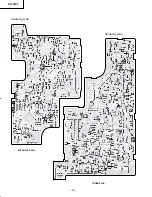

KH-WS1
– 30 –
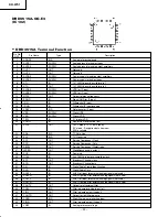
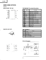
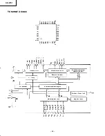
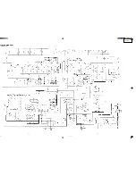
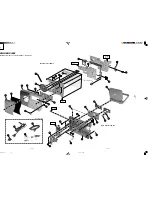
WIRING DIAGRAM
ANT PWB
W001
PG001
(MX)
CN204
(MX)
CN002
(MX)
PG002
(MX)
PG301
(MX)
PG303
(MX)
PG302
(PH)
PG202 (PH)
CN301 (MX)
Shield
Sheet
White
CN302
(PH)
CN303
(MX)
CN304
(TXL)
W302
SP001
PG201
(PH)
PG204
(PH)
PG304
(TXL)
PG203
(PH)
TUNER
FR
ONT END
RF101
H.P PWB ASS
LCD
DISPLA
Y PWB ASS
(patter
n
side vie
w
)
JK101
CN203
(PH)
CN201(PH)
IC201
S201
SA
T
. PWB ASS
L206 (FERRITE ANT)
TUNER PWB ASS
CT204
ø
1.0
T
e
rm
inal
DC
J
CN001
BA
TT CASE
BLK
T
w
isted
ORG
Z001
Add man
ual
solder
Batter
y
spr
ing
Solder after 1~2T
Winding of conductor par
t
to batter
y
spr
ing
CA
UTION:
Do not drop solder inside
speak
er or produce solder
spik
es when solder
ing this wire
.
3
1
2
1
1~2T Winding
of
insulation par
t
AC
INLET
PS PWB ASS
P,
T
Non colour
Bend wire
bef
ore
inser
tion
Bend wire
bef
ore
inser
tion
BLK RED
Gnd
Blue
L2
L1
–
+
KH/Pg 18-30 (IC chips)
10/11/00, 1:52 PM
30
Summary of Contents for KHWS1W
Page 5: ...KH WS1 5 Fig 4 Fig 5 5 6 ...
Page 6: ...KH WS1 6 Fig 6 Fig 7 metal pin 7 8 Connector J 9 ...
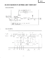
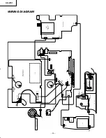
Page 17: ...KH WS1 17 BLOCK DIAGRAM OF ANTENNA AND TUNER UNIT Antenna Unit RF001 Tuner Unit RF101 ...
Page 26: ...KH WS1 26 TA7368P IC206 207 BU4066BCF IC204 BA033ST V5 IC209 1 9 7 8 1 14 1 2 3 4 5 ...
Page 28: ...KH WS1 28 TC9298F IC302 ...
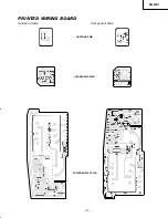
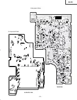
Page 32: ...KH WS1 32 SATELLITE P W B TUNER PWB Soldering Side Soldering Side ...
Page 33: ...KH WS1 33 Component Side TUNER PWB SATELLITE P W B Component Side ...
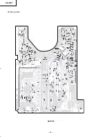
Page 34: ...KH WS1 34 Soldering Side MAIN PWB ...
Page 35: ...KH WS1 35 MAIN P W B Component Side ...
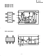
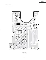
Page 37: ...KH WS1 CIRCUIT DIAGRAM TUNER DTS Circuit 38 37 it A2 10 11 00 1 57 PM 37 ...
Page 38: ...CIRCUIT DIAGRAM ATELLITE Circuit 40 39 it A2 10 11 00 1 57 PM 38 ...
Page 39: ...KH WS1 42 41 BLOCK DIAGRAM Lk Xploded A3 10 11 00 2 00 PM 41 ...
Page 41: ...THE UPDATED PARTS LIST FOR THIS MODEL IS AVAILABLE ON ESTA ...


