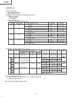
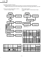
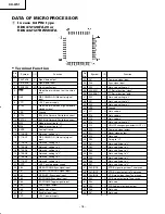
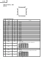
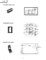
KH-WS1
– 20 –
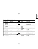
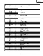
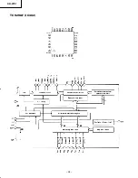
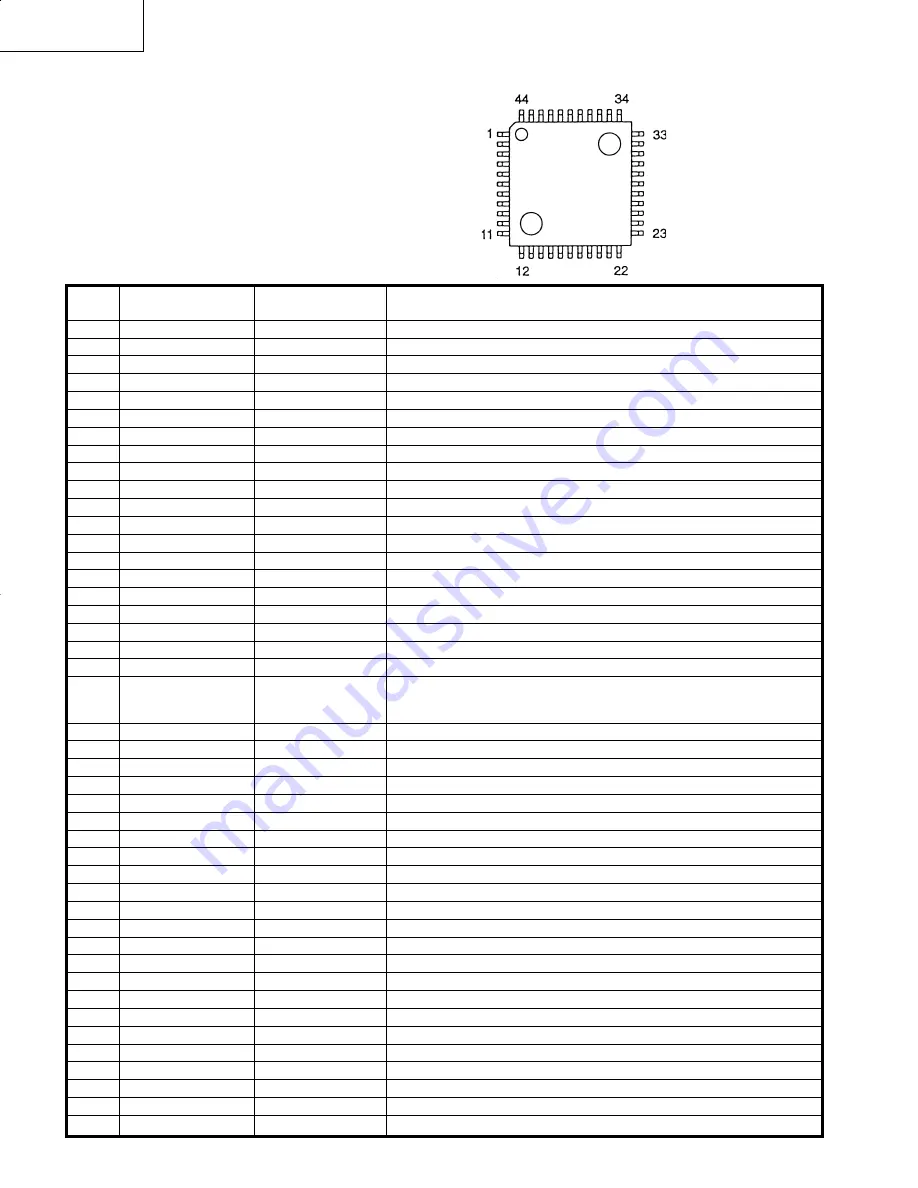
Pin No.
Pin Name
Type
Description
QFP
1
AGNDC
BID
Analog reference ground
2
AVSS1
SUPPLY
Analog ground for audio stages
3
AVSS0
SUPPLY
Analog ground for audio output amplifiers
4
OUT1
OUT
Not used
5
OUT2
OUT
Not used
6
AVDD0
SUPPLY
Power supply for audio output amplifiers
7
AVDD1
SUPPLY
Power supply for audio stages
8
XTI
IN
14.725 MHz quartz oscillator pin 1
9
XTO
OUT
14.725 MHz quartz oscillator pin 2
10
AVDD2
SUPPLY
VDD for IF input
11
AVSS2
SUPPLY
VSS for IF input
12
RCLK
OUT
Output reference frequency
13
SGND
IN
Signal GND for IF input
14
IFIN
IN
Differential IF input
15
IFINQ
IN
Differential IF input inverted
16
VREFI
BID
Reference for IF input
17
VSS
SUPPLY
Digital VSS
18
VDD
SUPPLY
Digital VDD
19
TEQ
IN
“H” digital VDD
20
PORQ
IN
Power On Reset, active low
21
SYNC
OUT
TSCC mode : TSCC data ready
BC mode : Decryption data from new
SCH available
22
SDA
BID
I
2
C Data Line
23
SCL
BID
I
2
C Clock Line
24
SCC
OUT
Service Component Clock
25
SCD
OUT
Service Component Data
26
SBCW
OUT
Service Component Wordstrobe
27
WSEN
OUT
WorldSpace enable output
28
PUP
IN
Power up
29
OCLK
IN
24.576 MHz input oversampling clock
30
BCC
OUT
Broadcast Channel clock
31
BCD
OUT
Broadcast Channel data
32
DAI
IN
Digital Audio Frame Identification
33
DAD
IN
Digital Audio Data
34
AUX2L
IN
AUX2 left input for external analog signals (not used)
35
AUX2R
IN
AUX2 right input for external analog signals (not used)
36
AUX1L
IN
AUX1 left input for external analog signals (not used)
37
AUX1R
IN
AUX1 right input for external analog signals (not used)
38
FOUTL
OUT
Output to left external filter
39
FOPL
BID
Filter op-amp inverting input, left
40
FINL
OUT
Filter op-amp output (line out)
41
FOUTR
OUT
Output to right filter op-amp
42
FOPR
BID
Right filter op-amp inverting input
43
FINR
OUT
Filter op-amp output (line out)
44
VREF
IN
Analog reference voltage
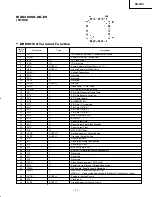
DRD3515A-QG-E3
(IC102)
•
DRD3515A Terminal Function
KH/Pg 18-30 (IC chips)
10/11/00, 1:52 PM
20
Summary of Contents for KHWS1W
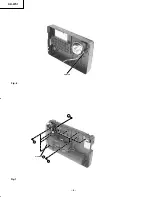
Page 5: ...KH WS1 5 Fig 4 Fig 5 5 6 ...
Page 6: ...KH WS1 6 Fig 6 Fig 7 metal pin 7 8 Connector J 9 ...
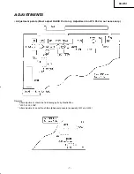
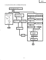
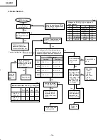
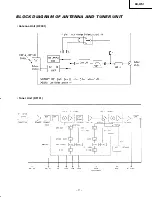
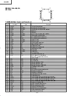
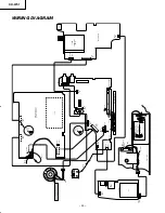
Page 17: ...KH WS1 17 BLOCK DIAGRAM OF ANTENNA AND TUNER UNIT Antenna Unit RF001 Tuner Unit RF101 ...
Page 26: ...KH WS1 26 TA7368P IC206 207 BU4066BCF IC204 BA033ST V5 IC209 1 9 7 8 1 14 1 2 3 4 5 ...
Page 28: ...KH WS1 28 TC9298F IC302 ...
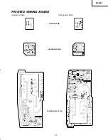
Page 32: ...KH WS1 32 SATELLITE P W B TUNER PWB Soldering Side Soldering Side ...
Page 33: ...KH WS1 33 Component Side TUNER PWB SATELLITE P W B Component Side ...
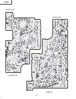
Page 34: ...KH WS1 34 Soldering Side MAIN PWB ...
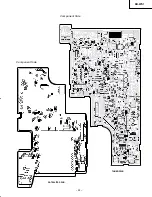
Page 35: ...KH WS1 35 MAIN P W B Component Side ...
Page 37: ...KH WS1 CIRCUIT DIAGRAM TUNER DTS Circuit 38 37 it A2 10 11 00 1 57 PM 37 ...
Page 38: ...CIRCUIT DIAGRAM ATELLITE Circuit 40 39 it A2 10 11 00 1 57 PM 38 ...
Page 39: ...KH WS1 42 41 BLOCK DIAGRAM Lk Xploded A3 10 11 00 2 00 PM 41 ...
Page 41: ...THE UPDATED PARTS LIST FOR THIS MODEL IS AVAILABLE ON ESTA ...