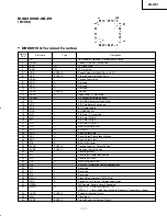
KH-WS1
– 12 –
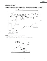
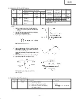
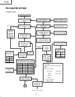
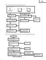
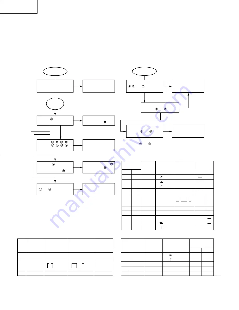
(2) Checking and flowchart for WS circuit
Determine the display on LCD and the presence or absence of sound from speakers after turning the power ON.
Note:
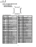
The terminal number of IC101is assumed 64-pin type in the flowchart. For 80-pin type, refer to tables 1 to 4 and note.
Start
No
Yes
WS
Function
Yes
Yes
Start
No
Yes
Yes
Note : 80 Pin
Type nos.
and
No
No
No
No
Is any sound output from
speakers when changing the
mode into RADIO?
Check the audio circuit
around IC206, IC207,
and IC210.
No
Check whether IC301
,
and
pin are in "H"
or not.
Check the terminals
of PG304 to IC101,
IC101 may malfunction.
No
Is the oscillator circuit of
IC101
and pin
in operation?
Check the oscillator
circuit or IC101 may
be in failure.
Is IC103
pin clocked in
at 14.725 MHz
Check R155 and
around IC103
pin.
Are
IC102 , , , pin
and
IC103 , , , pin
followed the table 3?
Check every port of
IC102 and IC103.
Is IC103
pin clocked
out at 24.576 MHz and
clocked into IC102
pin?
Check around IC102
pin and IC103
pin,
IC103 may malfunction.
Are the operations of IC103
and
pin followed the
table 4?
Check around IC103,
IC103 may malfunction.
Is any clock signal found in
IC101
and pin?
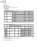
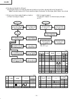
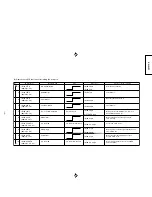
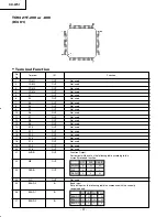
Table 2
Table 3
Table 4
H
H
H
H
H
H
H
IC101 No.
64 Pin
80 Pin
Power Off
(STANDBY)
Power Off
(STANDBY)
Power On
(NO BEAM)
Power On
(NO BEAM)
At receive
At receive
Connect to
another IC
Connect to
another IC
28
36
29
37
30
38
32
40
33
41
41
42
43
46
47
53
54
58
59
52
L
L
L
L
L
L
L
L
L
L
L
L
L
L
L
L
L
L
(reset)
H
L (reset)
H
H
L
L
L
L
L
(reset)
H
L (reset)
H
L (reset)
Sync Pulse
Data signal
Data signal
Data signal
Clock signal
Clock signal
27
21
26
25
24
28
20
IC102
IC103
7
41
40
39
2
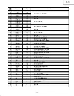
IC102
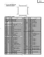
No.
Power Off
(STANDBY)
Power On
(NO BEAM)
At receive
Connect to
IC 101 No.
IC102
No.
30
31
32
33
16
22
23
27
33
L
L
L
L
L
L
L
L
H
L
H
L
H
27
26
25
24
23
35
64 Pin
80 Pin
33
32
30
28
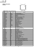
IC103 No.
24 kHz
Digital audio data
8 kHz
32
30
25
24
H
L (Sync puls)
H
L (Sync puls)
1
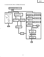
When no sound from speakers though any trouble is
not found in receiving and display
2
When no operation goes on
Only the part C of figure 1 or abnormal display will appear
on LCD.
KH/Pg 10-17 (TroubleSht)
10/11/00, 1:50 PM
12
Summary of Contents for KHWS1W
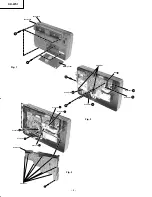
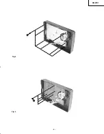
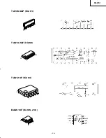
Page 5: ...KH WS1 5 Fig 4 Fig 5 5 6 ...
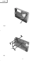
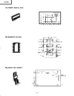
Page 6: ...KH WS1 6 Fig 6 Fig 7 metal pin 7 8 Connector J 9 ...
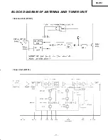
Page 17: ...KH WS1 17 BLOCK DIAGRAM OF ANTENNA AND TUNER UNIT Antenna Unit RF001 Tuner Unit RF101 ...
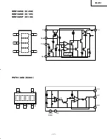
Page 26: ...KH WS1 26 TA7368P IC206 207 BU4066BCF IC204 BA033ST V5 IC209 1 9 7 8 1 14 1 2 3 4 5 ...
Page 28: ...KH WS1 28 TC9298F IC302 ...
Page 32: ...KH WS1 32 SATELLITE P W B TUNER PWB Soldering Side Soldering Side ...
Page 33: ...KH WS1 33 Component Side TUNER PWB SATELLITE P W B Component Side ...
Page 34: ...KH WS1 34 Soldering Side MAIN PWB ...
Page 35: ...KH WS1 35 MAIN P W B Component Side ...
Page 37: ...KH WS1 CIRCUIT DIAGRAM TUNER DTS Circuit 38 37 it A2 10 11 00 1 57 PM 37 ...
Page 38: ...CIRCUIT DIAGRAM ATELLITE Circuit 40 39 it A2 10 11 00 1 57 PM 38 ...
Page 39: ...KH WS1 42 41 BLOCK DIAGRAM Lk Xploded A3 10 11 00 2 00 PM 41 ...
Page 41: ...THE UPDATED PARTS LIST FOR THIS MODEL IS AVAILABLE ON ESTA ...