KH-WS1
– 24 –
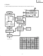
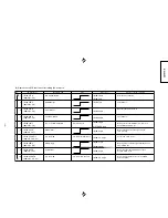
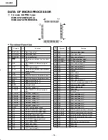
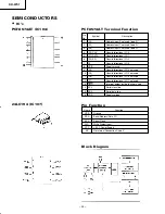
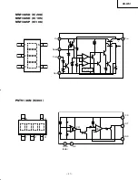
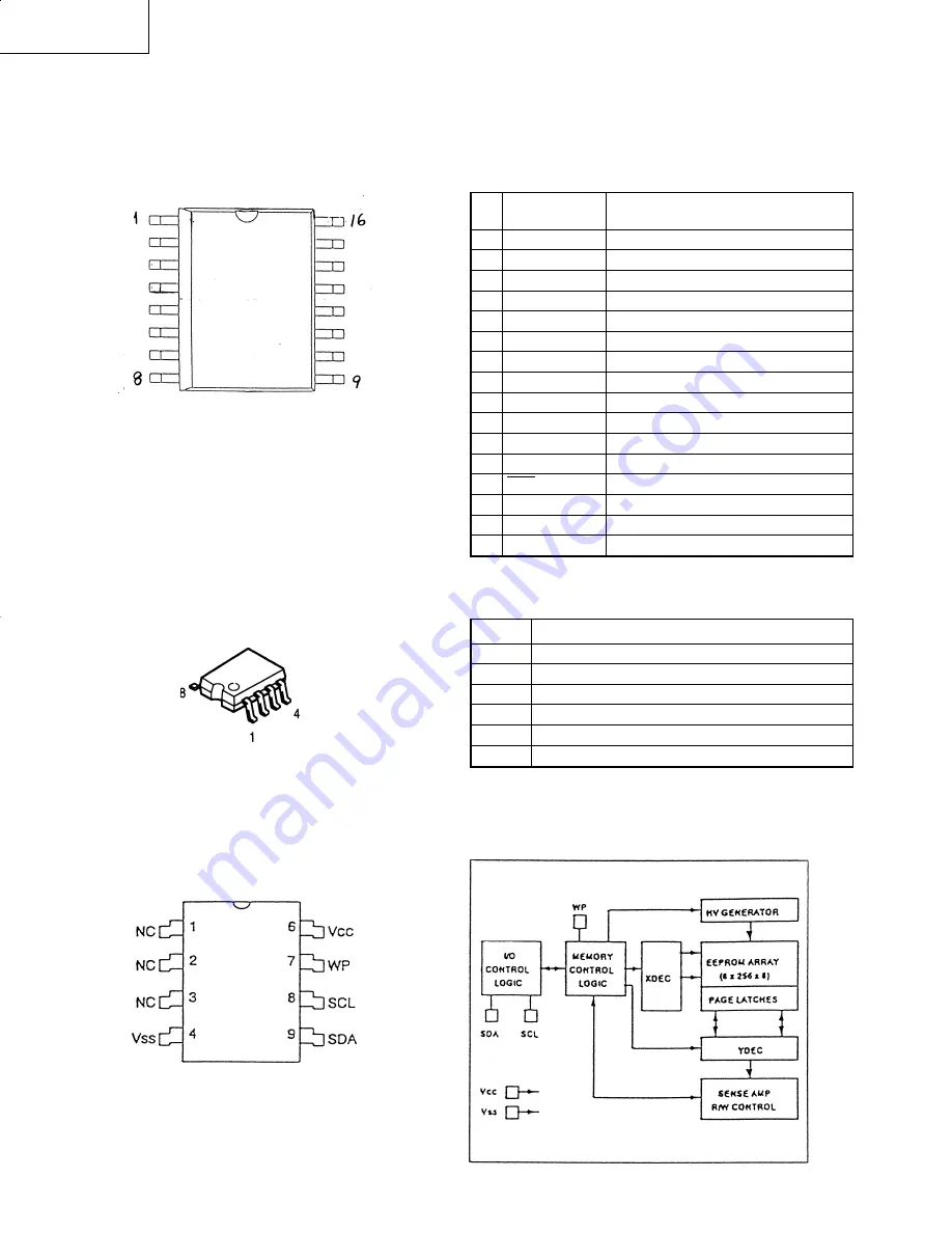
Pin
Symbol
Description
No.
1
(AO)
Address input 0 not used fixed “H”
2
(A1)
Address input 1 not used fixed “H”
3
(A2)
Address input 2 not used fixed “H”
4
(P0) CLK
Quasi-bidirectional I / O 0
5
(P1) DATA
Quasi-bidirectional I / O 1
6
(P2) EN
Quasi-bidirectional I / O 2
7
P3
Quasi-bidirectional I / O 3
8
VSS
Supply ground
9
(P4)
Quasi-bidirectional I / O 4 not used
10
(P5)
Quasi-bidirectional I / O 5 not used
11
(P6)
Quasi-bidirectional I / O 6 not used
12
(P7)
Quasi-bidirectional I / O 7 not used
13
(INT)
Interrupt output (active low) not used
14
SCL
Serial clock line
15
SDA
Serial data line
16
VDD
Supply voltage
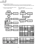
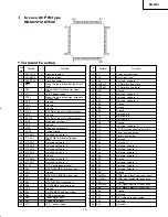
Pin Function
Name
Function
VSS
Ground
SDA
Serial Address/Data I / O
SCL
Serial Clock
WP
Write Protect Input
VCC
+3.2
∇
Power Supply
NC
No Internal Connection Fixed “L”
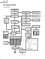
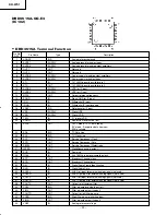
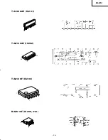
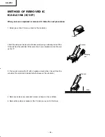
SEMICONDUCTORS
•
IC’s
PCF8574AT Terminal Function
Block Diagram
PCF8574AT (IC104)
24LC194 (IC107)
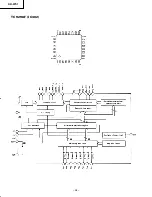
KH/Pg 18-30 (IC chips)
10/11/00, 1:52 PM
24
Summary of Contents for KHWS1W
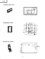
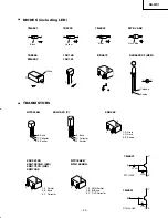
Page 5: ...KH WS1 5 Fig 4 Fig 5 5 6 ...
Page 6: ...KH WS1 6 Fig 6 Fig 7 metal pin 7 8 Connector J 9 ...
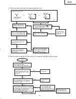
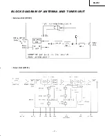
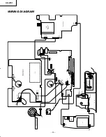
Page 17: ...KH WS1 17 BLOCK DIAGRAM OF ANTENNA AND TUNER UNIT Antenna Unit RF001 Tuner Unit RF101 ...
Page 26: ...KH WS1 26 TA7368P IC206 207 BU4066BCF IC204 BA033ST V5 IC209 1 9 7 8 1 14 1 2 3 4 5 ...
Page 28: ...KH WS1 28 TC9298F IC302 ...
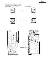
Page 32: ...KH WS1 32 SATELLITE P W B TUNER PWB Soldering Side Soldering Side ...
Page 33: ...KH WS1 33 Component Side TUNER PWB SATELLITE P W B Component Side ...
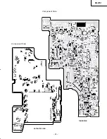
Page 34: ...KH WS1 34 Soldering Side MAIN PWB ...
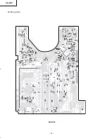
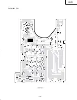
Page 35: ...KH WS1 35 MAIN P W B Component Side ...
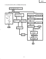
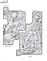
Page 37: ...KH WS1 CIRCUIT DIAGRAM TUNER DTS Circuit 38 37 it A2 10 11 00 1 57 PM 37 ...
Page 38: ...CIRCUIT DIAGRAM ATELLITE Circuit 40 39 it A2 10 11 00 1 57 PM 38 ...
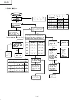
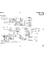
Page 39: ...KH WS1 42 41 BLOCK DIAGRAM Lk Xploded A3 10 11 00 2 00 PM 41 ...
Page 41: ...THE UPDATED PARTS LIST FOR THIS MODEL IS AVAILABLE ON ESTA ...