background image

KH-WS1

– 11 –

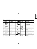
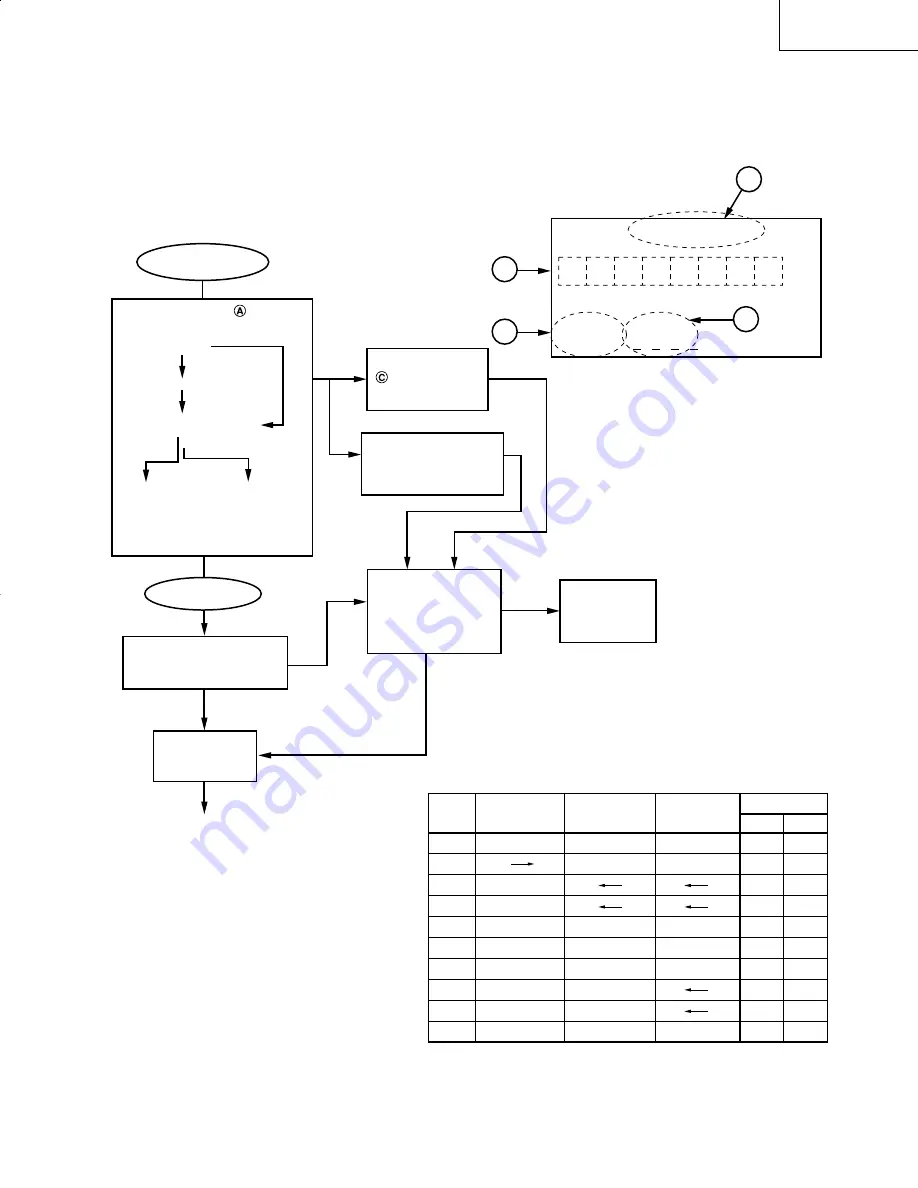
WS Function

No

No

No

Yes

LCD Display

A

WS

 (SC)

LEVEL

1

STEREO LOCKED

W S

S A T

Yes

Yes

Yes

Yes

At receiving

WS SAT

"SEARCH"

AFRST–1

NO BEAM
(when no signal
received)

Display
Broadcast name
(when any
signal received)

– 1

*

or

eg)

or

C

B

B

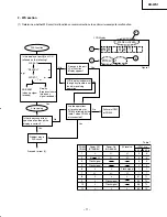
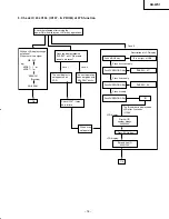
Is the display of part 

 on LCD

followed on the following?

Is there any sound from
speakers even though the
display is correct?

Problem may in

WS circuit.

Proceed to item (2).

Does only the part


  of Function

display appear?

LCD display is abnormal
though any trouble is not
found in receiving
operation.

Are the operations
of terminal pins for
CN304 followed on the
table 1 when CN304 is
disconnected?

Failure in IC301
or CN304

Figure 1

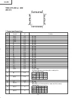
PG304
CN304

1

L

H

H

5

5

2

(L)         H

H

H

4

4

3

Clock signal

3

3

5

Clock signal

2

2

6

L

L

Clock signal

1

1

7

H

H

H

7

7

8

L

L

L

57

71

9

L

Clock signal

59

74

10

L

Clock signal

58

72

11

L

L

L

60

75

Power Off

(STANDBY)

Power On

(NO BEAM)

At receive

IC101 No.

64 Pin 80 Pin

Table 1

2. WS section

(1) Determine whether WS circuit malfunctions or communications to control microcomputer malfunction.

KH/Pg 10-17 (TroubleSht)

10/11/00, 1:50 PM

11

Summary of Contents for KHWS1W

Page 1: ...ons for management export and supply to overseas based on the Wassenaar Arrangement CONTENTS SPECIFICATIONS 2 SERVICE POINTS 3 ADJUSTMENTS 7 TROUBLESHOOTING 10 BLOCK DIAGRAM OF ANTENNA AND TUNER UNIT 17 DATA OF MICROPROCESSOR 18 SEMICONDUCTORS 24 WIRING DIAGRAM 30 PRINTED WIRING BOARD 31 METHOD OF REMOVED IC 36 CIRCUIT DIAGRAM 37 BLOCK DIAGRAM 41 EXPLODED VIEW 43 REPLACEMENT PARTS LIST 45 ...

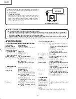
Page 2: ... 9 500 26 100 MHz Meter band 31 25 21 19 16 13 11 m Antennas FM SW1 SW2 Telescopic antenna aerial MW Built in ferrite core antenna aerial General Specifications Power supply AC 110 127 V 220 240 V 50 60 Hz DC 6 V D cell or IEC R20 or equivalent x 4 Optional DC input jack Input voltage DC 6 V 30 10 DC 7 8 V 5 4 V Current consumption max 400 mA Power mains consumption 5 W Audio output 3 W PMPO 300 m...

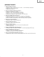
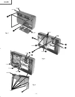
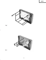
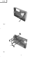
Page 3: ...ve 1 screw 5 from the Tuner P W B Board 3 Detach 9 catches and separate the Tuner P W B Board from the sub chassis 3 Removal of Insulator Pad Fig 4 1 Remove 6 screws 5 from the Insulator pad 4 Removal of Main Board Fig 5 1 Remove 4 screws 6 from the Main Board 5 Removal of Speaker Fig 6 1 Release one end of the metal pin that secures the speaker position 2 Slide out the speaker 6 Removal of POWER ...

Page 4: ...4 Fig 3 5 9 Catches Connector H Connector Sub Chassis I Connector E Connector F Connector G Fig 1 Fig 2 1 2 Back case Front case Battery cover 4 Connector 3 Catches Ant 3 A Connector B Connector C Connector D ...

Page 5: ...KH WS1 5 Fig 4 Fig 5 5 6 ...

Page 6: ...KH WS1 6 Fig 6 Fig 7 metal pin 7 8 Connector J 9 ...

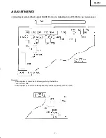
Page 7: ...oints Must adjust RADIO Part only Adjustment on WS Part is not necessary Remarks After adjustment should be fix following parts by Electro Wax L201 L202 L206 After adjustment do not touch the alighed components especially L201 and L202 ...

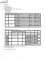
Page 8: ...eat step 1 2 1 9 5 MHz L209 1 6 V 0 1 2 26 1 MHz CT206 9 0 V 0 3 3 Repeat step 1 2 Remarks Instrument Connection 1 With a 470 µF 6 3 V capacitor to the TP2 and J209 B IC202 2 Mean Note 2 See page 17 Note AM TRACKING ERROR SPEC 6dB Step Item 1 AM IF 2 1 MW Ant 2 3 3 1 SW1 Ant 2 3 4 1 SW2 Ant 2 3 Required Instrument Connection Instrument Input Output Genescope 1 Ferrite Ant 2 TP1 AM signal generator...

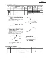
Page 9: ...nna is shown in Fig 3 6 FM dummy antenna is shown in Fig 4 R1 Rg SG s output impedance 75 Ω R2 75 Rg 2 5 Alignment for Clock Time Accuracy Step Item 1 IF 2 1 FM 2 3 Required Instrument Connection Instrument Input Output Genescope IC201 TP1 Note 3 FM signal P1 TP1 Generator 400 Hz 22 5 kHz Dev Note 6 Genescope or Receiving Adjust Reading SG Freq Freq Set 10 7 MHz High End or T201 Max 106 1 MHz Freq...

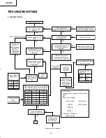
Page 10: ... Is the LCD display followed the right table Check and follow the flowchart for each functions Proceed to each flowchart Is the voltage to the Voltage Selector set correctly Disconnect the power cord and set the voltage correctly Check the 3 V line Check the oscillator circuit or IC301 is broken down Check BATT display Is BATT blinking on the LCD Check Q302 307 and D318 CN302 Pin IC301 Pin 4 2V BA...

Page 11: ...part of Function display appear LCD display is abnormal though any trouble is not found in receiving operation Are the operations of terminal pins for CN304 followed on the table 1 when CN304 is disconnected Failure in IC301 or CN304 Figure 1 PG304 CN304 1 L H H 5 5 2 L H H H 4 4 3 Clock signal 3 3 5 Clock signal 2 2 6 L L Clock signal 1 1 7 H H H 7 7 8 L L L 57 71 9 L Clock signal 59 74 10 L Cloc...

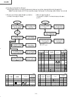
Page 12: ...C102 pin Check around IC102 pin and IC103 pin IC103 may malfunction Are the operations of IC103 and pin followed the table 4 Check around IC103 IC103 may malfunction Is any clock signal found in IC101 and pin Table 2 Table 3 Table 4 H H H H H H H IC101 No 64 Pin 80 Pin Power Off STANDBY Power Off STANDBY Power On NO BEAM Power On NO BEAM At receive At receive Connect to another IC Connect to anoth...

Page 13: ...03 pin operate in L Check around the terminals of IC103 and IC101 When the stations receivable with other units can not be received though the operation is proper Execute SEEK Search Push MODE and BEAM SEEK keys Can IC101 pin switch H to L after starting SEEK until it ends 80 pin Check IC101 Check IC105 and IC106 Check the output line of IC105 and IC106 and around the terminals of RF101 Does the v...

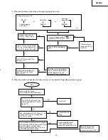
Page 14: ... Check to confirm operation WS RESET Output Reset IC102 and IC103 DCEN Output PUP IN Input PUP OUT Output Clock 14 725 MHz Output WRDY Input I2 C BUS I O WSEN Input SYNC Input I2 C BUS I O I2 C BUS communication I2 C BUS communication Clock waveform Turn IC103 on Make sure IC103 is turned on Turn IC102 on IC103 generates 24 576 MHz from this clock 14 725MHz for 38 pin out IC103 outputs a verificat...

Page 15: ...es Case 1 Case 2 Case 3 The next display is not appeared on LCD The next operation does not go on with SEARCH blinks Push MODE Key Turn on light MODE Push PASSWORD Key Push PASSWORD Key Push PASSWORD Key ID PASSW 02 PASSW 01 Check IC107 it may be in failure When it can not operate Description of LCD display Press it successively Press it secondly Press it thirdly The ID number is displayed on LCD ...

Page 16: ... circuits for RADIO parts Cause of malfunction Are the voltages for PG302 and pin followed on the table 6 when CN302 is disconnected Check the circuits G and H of S201 Check IC301 Is the voltage for Q219 collector followed on the next table when its frequency is up and down High end Low end frequency Can the indication of LOCKED light Check the audio circuits of IC205 IC206 IC207 and IC210 Check I...

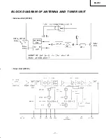
Page 17: ...KH WS1 17 BLOCK DIAGRAM OF ANTENNA AND TUNER UNIT Antenna Unit RF001 Tuner Unit RF101 ...

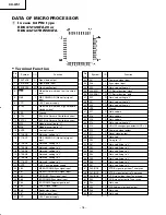
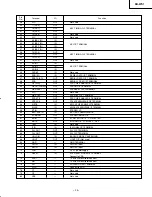
Page 18: ... signal output 29 P66 I Ready signal input 30 P67 O Enable signal input 31 VCC 3 2 power supply Pin Symbol I O Function No 32 P27 I Power up signal input 33 P26 I Sync signal input 34 P25 I Not used setting to L 35 P24 SCL1 O I 2 C Serial bus line clock 36 P23 SDA1 O I 2 C Serial bus line data 37 P22 O Not used setting to L 38 P21 O Not used setting to L 39 P20 O Not used setting to L 40 VSS Groun...

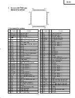
Page 19: ...al input 36 P65 O DCEN signal output 37 P66 I Ready signal input 38 P67 O Enable signal input 39 VCC 3 2 power supply Pin Symbol I O Function No 40 P27 I Power up signal input 41 P26 I Sync signal input 42 P25 I Not used setting to L 43 P24 SCL1 O I 2 C Serial bus line clock 44 P23 SDA1 O I 2 C Serial bus line data 45 VSS Ground 46 P22 O Not used setting to L 47 P21 O Not used setting to L 48 P20 ...

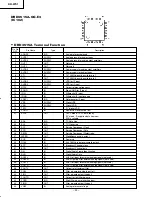
Page 20: ...from new SCH available 22 SDA BID I 2 C Data Line 23 SCL BID I 2 C Clock Line 24 SCC OUT Service Component Clock 25 SCD OUT Service Component Data 26 SBCW OUT Service Component Wordstrobe 27 WSEN OUT WorldSpace enable output 28 PUP IN Power up 29 OCLK IN 24 576 MHz input oversampling clock 30 BCC OUT Broadcast Channel clock 31 BCD OUT Broadcast Channel data 32 DAI IN Digital Audio Frame Identifica...

Page 21: ...I13 O MPEG FRAME SYNC 23 PI12 O BC SYNC 24 SOD O Serial Output Data 25 SOI O Serial Output Frame Identification 26 SOC O Serial Output Clock 27 PI8 O MPEG CRC Error 28 XVDD SUPPLY Positive Supply of Output Buffers 29 XVSS SUPPLY Ground of Output Buffers 30 SID I Serial Input Data 31 SII I Serial Input Frame Identification 32 SIC I Serial Input Clock 33 PI4 O MPEG FRAME SYNC 34 PI3 I AUD SW informa...

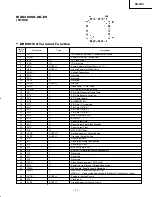
Page 22: ...12 OUT Not used 17 S 13 OUT Not used 18 S 14 OUT Not used 19 S 15 OUT Not used 20 S 16 OUT Not used 21 AUDIO OUT Function Output Port output will be set as the following table according to the currently received function 22 WS OUT 23 RADIO OUT 24 N C OUT Not used 25 BAND 0 IN Band Input Set port input as the following table in accordance with the currently receiving band 26 BAND 1 IN 27 BAND 2 IN ...

Page 23: ... 54 DTS STB OUT DTS CHIP ENABLE O P TERMINAL 55 DTS ACK OUT DTS ACKNOWLEDGE O P TERMINAL 56 M STB IN MICON CHIP ENABLE I P TERMINAL 57 M ACK IN MICON ACKNOWLEDGE I P TERMINAL 58 ST IN IN STEREO I P 59 BATTERY IN IN BATTERY REMAINING I P 60 ST MONO OUT STEREO MONO O P 61 SD IN IN ST DETECTION I P L DETECTED 62 MUTE OUT MUTING O P H MUTE L OFF 63 TEST IN Not used 64 IF IN IN IF SIGNAL I P TERMINAL 6...

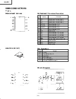
Page 24: ...bidirectional I O 4 not used 10 P5 Quasi bidirectional I O 5 not used 11 P6 Quasi bidirectional I O 6 not used 12 P7 Quasi bidirectional I O 7 not used 13 INT Interrupt output active low not used 14 SCL Serial clock line 15 SDA Serial data line 16 VDD Supply voltage Pin Function Name Function VSS Ground SDA Serial Address Data I O SCL Serial Clock WP Write Protect Input VCC 3 2 Power Supply NC No ...

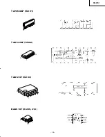
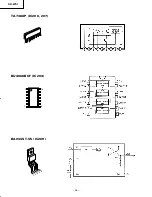
Page 25: ...KH WS1 25 TA7358AP IC201 1 9 TA8132AF IC202 TA8126F IC203 BA4510F IC205 210 1 12 24 1 5 10 1 8 4 ...

Page 26: ...KH WS1 26 TA7368P IC206 207 BU4066BCF IC204 BA033ST V5 IC209 1 9 7 8 1 14 1 2 3 4 5 ...

Page 27: ...KH WS1 27 MM1385D IC208 MM1385H IC105 MM1385P IC106 PST9136N IC303 1 2 3 5 4 5 4 2 Vin Vout Noise Cont Gnd T h e r m a l P r o t e c t 3 1 5 1 2 3 4 C01 OPI VCC OUT GND N C GND 5 4 3 1 2 SUB ...

Page 28: ...KH WS1 28 TC9298F IC302 ...

Page 29: ... Emitter 2 1 1 D Drain 2 G Gate 3 S Source 3 2 1 1 E Emitter 2 B Base 3 C Collector 3 2 1 1 E GND Emitter 2 B IN Base 3 C OUT Collector 3 B DTC124EK 22 kΩ 22 kΩ C E B DTA144GKA 47 kΩ C E 1SS133 1N4001 MTZ J3 6B 1SS355 FM4002 1SV149 1SV101 RB461F SLR56VC3F RED HIT9016G 2SA1020 Y 2SK242 2SC2412K 2SA1037AK Q R 2SD1757K Q R 2SD1048 DTC124EK DTA144GKA 1N4531 1N4531 ...

Page 30: ...view JK101 CN203 PH CN201 PH IC201 S201 SAT PWB ASS L206 FERRITE ANT TUNER PWB ASS CT204 ø1 0 Terminal DC J CN001 BATT CASE BLK Twisted ORG Z001 Add manual solder Battery spring Solder after 1 2T Winding of conductor part to battery spring CAUTION Do not drop solder inside speaker or produce solder spikes when soldering this wire 3 1 2 1 1 2T Winding of insulation part AC INLET PS PWB ASS P T Non ...

Page 31: ...KH WS1 31 PRINTED WIRING BOARD Soldering Side POWER SUPPLY PWB Component Side HEADPHONE PWB ANTENNA PWB ...

Page 32: ...KH WS1 32 SATELLITE P W B TUNER PWB Soldering Side Soldering Side ...

Page 33: ...KH WS1 33 Component Side TUNER PWB SATELLITE P W B Component Side ...

Page 34: ...KH WS1 34 Soldering Side MAIN PWB ...

Page 35: ...KH WS1 35 MAIN P W B Component Side ...

Page 36: ...e have a tweezers on hand to pick up the IC 3 Pick up and remove the IC with a tweezers slowly when it travels from the substrate Be careful not to delaminate the traces on the substrate 4 Remove and clean any redundant solders on traces on the substrate 5 Remove the solders on leaders of the IC when you reuse it in the future Solders Tweezer Soldering iron Tweezer PWB When you reuse a replaced or...

Page 37: ...KH WS1 CIRCUIT DIAGRAM TUNER DTS Circuit 38 37 it A2 10 11 00 1 57 PM 37 ...

Page 38: ...CIRCUIT DIAGRAM ATELLITE Circuit 40 39 it A2 10 11 00 1 57 PM 38 ...

Page 39: ...KH WS1 42 41 BLOCK DIAGRAM Lk Xploded A3 10 11 00 2 00 PM 41 ...

Page 40: ...ase Assembly Accessories Front Case Assembly 7 41 44 32 31 34 39 9 40 37 28 30 36 42 43 7 8 38 29 33 3 19 20 5 6 26 22 17 12 14 16 24 23 10 11 13 25 15 27 18 21 35 TUNER PWB ASSY ANTENNA PWB PS PWB ASSY KEY PWB ASSY SAT PWB ASSY 44 43 Lk Xploded A3 10 11 00 2 00 PM 42 ...

Page 41: ...THE UPDATED PARTS LIST FOR THIS MODEL IS AVAILABLE ON ESTA ...

Page 42: ... ITALY Tel 39 02 487861 Tel 39 02 38073415 Servizio Clienti Fax 39 02 48786381 2 Email customerservice italy hitachi eu com HITACHI Europe AB Box 77 S 164 94 Kista SWEDEN Tel 46 0 8 562 711 00 Fax 46 0 8 562 711 13 Email csgswe hitachi eu com HITACHI EUROPE S A S Lyon Office B P 45 69671 BRON CEDEX FRANCE Tel 04 72 14 29 70 Fax 04 72 14 29 99 Email france consommateur hitachi eu com HITACHI EUROPE...

Reviews: