


32
The oscillator consists of the control gate, two inverters and an RC network which determines the
operating frequency. Variable resistor P1 permits adjustment of the frequency. The output of the oscillator
(pin 10 of IC-24) drives the base of a current amplifier transistor, Q4. The output signal is developed across
the collector load resistor, P302, which controls the level fed to the speaker and, through an isolating
capacitor, to the audio output jack.
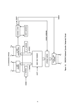
4.14 Quick Brown Fox Generator and ID Control
The purpose of the quick brown fox (QBF) generator is to produce the standard RTTY test message (The
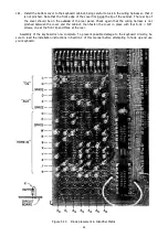
quick brown fox jumps over the Lazy dog's back Ø123456789) with a single keystroke. The circuit, shown in
Figure 8.12, also includes logic to control the operation of the identifier and the three-character sequencers,
to be described in later sections.
The QBF test message characters are stored in two sections of the ROM code converter, each containing
32 addresses. The remaining six sections of the ROM store the RTTY and Morse codes for each ASCII
character supplied by the keyboard encoder. When the QBF generator is active, the keyboard is disabled
and the address input of the ROM (data lines A
0
through A
7
) is driven by the QBF generator instead.
The generator's character sequence is controlled by a six-bit counter. The output of the five least
significant stages are coupled through diodes to data lines A
0
through A
4
. Lines A
5
and A
6
, used in normal
RTTY operation to signal control functions, are driven low for the entire time the generator is active. The A
7
line, which normally selects the Morse or the RTTY portion of the ROM, is connected to the most significant
counter stage. When the generator has been activated, the counter increments through its 64 states. During
the first 32 states, the storage locations in the first of the two ROM QBF sections are addressed sequentially
by the counter output, producing the first half of the test message. On the 32nd input pulse, the A
7
line
changes state and selects the second of the two QBF sections. The next 32 characters then appear at the
ROM output as the counter increments.
The generator cycle is initiated when the QBF key is pressed, pulling the
QUICK BROWN FOX START
line
low. If the mode switch is set for RTTY operation, the M/R line is low also. Both signals are coupled to the
input of a NOR gate (pins 2 and 3 of IC-54). With the key pressed, both inputs are low and the output,
coupled to a gate at the clear terminals of the first four counter stages, goes high. The other gate input is
connected to the
ID ACTIVE
line. If either the identifier or one of the three-character sequencers is active,
the line is low, preventing the QBF counters from resetting. If, on the other hand, the
ID ACTIVE
line is
high, the QBF counter reset terminals are allowed to go high and the counter is reset. Note that the clear
terminals of the two most significant stages are driven by a separate NAND gate (pins 3, 4, and 5 of IC-52).
These stages reset when their clear terminals are driven Low.
The Q output of each counter stage is coupled to an input of a NAND gate (IC-51). When the counter
has cycled through all of its 64 states, all inputs to the gate are high and its output is low. The circuit
remains in this state until the next time the test sequence is initiated. As soon as the QBF key closes, the
counter resets, and the output of IC-51 goes high. This signal is coupled through another NAND gate whose
output (pin 8 of IC-52) is combined with the
HERE IS ACTIVE
line and the inverted THREE LETTER GROUP
ACTIVE line in a four-input NAND gate.
The output of the latter gate (pin 6 of IC-44) drives the
ENABLE KEYBOARD
line. If any of the automatic
character string generators is active, the
ENABLE KEYBOARD
line goes high. Fed back to the buffer control
circuit, this signal prevents the keyboard encoder from producing character codes until the character string
has been completed.
When the counters have been reset by closure of the QBF key and the
ENABLE KEYBOARD
line has gone
high, the
ID ACTIVE
line is driven low. Since the latter signal is coupled to the NAND gate at the counter
clear terminals, its transition removes the clear command produced by the QBF key closure and the counter
is free to toggle as pulses reach its input stage.
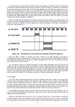
Clock pulses are supplied to the counter from the buffer control circuit via the
RESUME ID
line, which
drives the
READY ID
line through a NAND gate. The gate is inhibited during normal keyboard operation,
since the
ENABLE KEYBOARD
line stays low, When any of the automatic sequencers is active, however, the
gate opens and pulses are allowed to flow to the counter.
Summary of Contents for DKB-2010
Page 1: ......
Page 20: ...18...
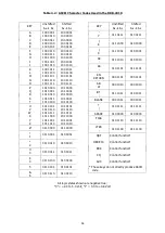
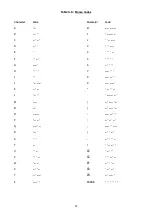
Page 39: ...37 Table 4 3 ROM Converter Input and Output Codes...
Page 52: ...50 Figure 6 1 Logic Circuit Board Test Points...
Page 53: ...51 Figure 6 2 Keyswitch Circuit Board Test Points...
Page 54: ...52 Figure 6 3 Power Supply Circuit Board Test Points...
Page 57: ...55 Table 6 4 DKB 2010 Wire List...
Page 63: ...61...
Page 64: ...62...
Page 65: ...63...
Page 67: ...65...
Page 69: ...67...
Page 71: ...69...
Page 73: ...71...
Page 75: ...73...
Page 77: ...75...
Page 79: ...77...
Page 81: ...79...
Page 83: ...81...
Page 85: ...83...
Page 87: ...85...
Page 89: ...87...
Page 91: ...89...
Page 92: ...90...
Page 93: ...91...
Page 94: ...92...
Page 95: ...93...
Page 96: ...A1 EXTENDED MEMORY OPTION FOR THE DKB 2010 KEYBOARD INSTRUCTION MANUAL...
Page 100: ...A5...
Page 101: ...A6...