


22
The output of each stage in the character timing counter is connected to one of the four inputs of a
NAND gate (IC-28). When the counter has received fifteen clock pulses, all of the gates inputs are high. The
output goes low, resetting the counter before the sixteenth clock pulse arrives. The reset signal is also fed
back to pin 11 of IC-14, stopping the flow of clock pulses to the
RTTY SHIFT
line. Clocking of the shift
register consequently stops at the end of the character. The reset signal is also returned to the RTTY run
flip-flop, returning it to the clear or "ready" state.
In the event that the new character is in a different case from the preceding one, the sequence of
operations is somewhat different. The keyboard must delay transmission of the new character until the
letters-case or figures-case code has been sent to change the receiving printer to the correct case. The case
code is not produced by the shift register; rather, it is generated by logic gates connected to the character
timing counter.
As mentioned in Section 4.5, the D
0
bit from the ROM code converter indicates the case of each
character produced. Applied to gates at the input of the case change flip-flop, it is combined with the LOAD
RTTY signal and the
D
7
bit. When the LOAD RTTY line goes high, indicating that a new character has
entered the shift register, and provided that the
D
7
bit is high, the D
0
bit passes through the NAND gates to
the inputs of the case change flip-flop, If the new character is of a different case than the preceding one,
the flip-flop changes states. The flip-flop outputs are dynamically coupled to the preset terminal of the case
insert flip-flop, forcing it to the set state. The INSERT CASE CODE Line is driven high, signaling the RTTY
encoder to accept an input from the case character generator rather than from the shift register.
An output from the
Q
or "0" terminal of the case insert flip flop closes the shift register clock gate,
preventing clock pulses from flowing to the register. The character stored in the register is therefore held
until the case-shift code has been transmitted.
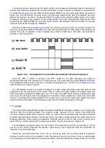
The character timing counter, however, is allowed to run as usual. Its output states are decoded by the
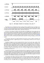
case character generator gates (IC-34) to produce the waveforms shown at the bottom of Figure 8.5.
Pin 6 of the gate is low during the "0" and "1" states of the counter, producing the
C = 0v1
output. Pin
12 is low during the sixth and seventh counts, driving the
C = 6v7
output low. The
C = 0v1
output by itself
is equivalent to the RTTY letters-shift code. When added to the
C = 6v7
output, it produces the figures-shift
code.
The two signals are fed to the RTTY encoder (Figure 8.7) along with outputs from the case change flip-
flop. The latter signals instruct the encoder which of the two case codes is to be generated. The RTTY
encoder then uses one or both of these two signals to key the loop and transmit the required case code.
The shift register remains dormant until the case-change character has been completed. At that time, the
character timing counter reaches its fifteenth state and the counter reset gate output goes low. This signal
resets the counter and the case insert flip-flop. A signal from the flip-flop's Q output, coupled to one input of
the NAND gate at the RTTY run flip-flop toggle terminal, prevents the latter flip-flop from being reset. It also
opens the shift register clock gate. The character timing counter, which is still receiving clock pulses, restarts
at the zero state, but this time clock pulses are allowed to flow to the shift register. As a result, the
character stored in the register is clocked out to the RTTY loop keying circuit.
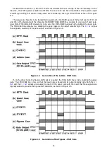
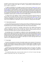
4.8 Shift Register and Control Circuit
Characters arriving from the storage buffer in parallel are converted to serial form by the shift register,
shown in Figure 8.6. The register consists of two IC's, each containing five flip-flops. The input code,
whether a Morse or RTTY character, is supplied to the register on data Lines D
0
through D
7
. Register
operation is controlled by the two flip-flops which comprise IC-7.
In the quiescent state, both the MORSE START and the RTTY START lines are low. These signals are
combined in the gates which make up IC-8, driving the output (pin 1) low. Coupled to the reset terminals of
the shift register stages, this output clears the register.
As soon as a character has been transferred from the keyboard encoder to the storage buffer, the
BUFFER FULL line goes high. On the next positive-going transition of the HØ clock, the first of the shift
register control flip-flops toggles, and its Q output drives the
BUFFER READ
line low. The same signal passes
Summary of Contents for DKB-2010
Page 1: ......
Page 20: ...18...
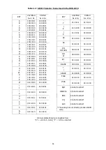
Page 39: ...37 Table 4 3 ROM Converter Input and Output Codes...
Page 52: ...50 Figure 6 1 Logic Circuit Board Test Points...
Page 53: ...51 Figure 6 2 Keyswitch Circuit Board Test Points...
Page 54: ...52 Figure 6 3 Power Supply Circuit Board Test Points...
Page 57: ...55 Table 6 4 DKB 2010 Wire List...
Page 63: ...61...
Page 64: ...62...
Page 65: ...63...
Page 67: ...65...
Page 69: ...67...
Page 71: ...69...
Page 73: ...71...
Page 75: ...73...
Page 77: ...75...
Page 79: ...77...
Page 81: ...79...
Page 83: ...81...
Page 85: ...83...
Page 87: ...85...
Page 89: ...87...
Page 91: ...89...
Page 92: ...90...
Page 93: ...91...
Page 94: ...92...
Page 95: ...93...
Page 96: ...A1 EXTENDED MEMORY OPTION FOR THE DKB 2010 KEYBOARD INSTRUCTION MANUAL...
Page 100: ...A5...
Page 101: ...A6...