


21
Buffer operation is controlled by the Logic circuit shown at the left in the drawing. When a new character
has been produced by the keyboard encoder, the READY line goes high. This signal passes through a NOR
gate where it is combined with the ID READY signal. Thus, if a character is ready at either the keyboard or
at the identifier, the output of the NOR gate will be low. This terminal is connected to the D input of the first
of a string of four flip-flops (IC's 1 and 2). The flip-flop clock terminals are driven by the HØ clock line. On
the first positive-going clock transition after the READY signal appears, the first flip-flop changes states,
driving pin 5 of circuit 2 low. If the
ENABLE KEYBOARD
bus is low, the signal passes through two NOR gates
and drives the
ENABLE
terminal of the encoder low, causing the new character to be transferred to the ROM
input. The converted character code appears at the output of the ROM, ready for loading into the storage
buffer.
Assuming that the buffer is free (that any previous character has been transferred from the buffer to the
shift register), the LOAD BUFFER lines, which drive the buffer register clock terminals, will be driven high on
the next positive clock transition. The data from the ROM, coupled to the D inputs of the buffer flip-flops,
then enters the buffer. On the next clock pulse, the LOAD BUFFER line goes low, preventing further
characters from entering until the current character has been transferred to the shift register. One clock
pulse later, the
ENABLE
line goes high, decoupling the keyboard encoder from the ROM input.
When a character is waiting in the buffer register, the last of the four flip-flops is set with its a output
high, driving the BUFFER FULL line high. After the contents of the buffer are read into the shift register, the
BUFFER READ
line is driven low by the shift register control circuitry, resetting the last two flip-flops in the
buffer control.
In the case where input data are being supplied to the ROM from the identifier rather than the keyboard,
it is necessary to inhibit the identifier sequence when the buffer is full, and to notify the identifier when the
buffer is ready to accept a new character. The signal fed to the identifier (and to the other automatic
sequencers as well) via the
RESUME ID
line serves this purpose. When the buffer is full, the line is driven
low. As soon as the character in the buffer has been accepted by the shift register, the
BUFFER READ
Line is
driven low, pulling the
RESUME ID
bus Low also. The identifier then passes a new character to the ROM
input, where it is converted and fed to the buffer.
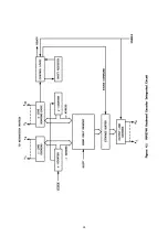
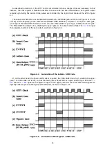
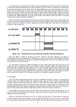
4.7 RTTY Control and Decoding Circuit
When the keyboard is set to the RTTY mode, the transfer of characters from the buffer to the shift
register, as well as the subsequent operation of the shift register, is supervised by the RTTY control circuit,
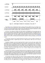
shown in Figure 8.5.
The control circuit is composed primarily of the RTTY run flip-flop (IC-15), the case change flip-flop, the
case insert flip-flop, and the character timing counter. The latter is a divide-by-16 counter coupled to control
gates which reset it to the zero state when a count of fifteen is reached. Its purpose is to control the
number of clock pulses reaching the shift register. It passes only enough pulses to clock out the RTTY start
pulse, the five character-code bits, and the stop pulse.
The clock input of the counter is driven at twice the baud rate for the RTTY operating speed chosen. The
clock pulse source is the 0 output of the RTTY timing chain (Figure 8.8).
Operation of the counter is controlled by the RTTY run flip-flop. Assume for the moment that the shift
register is idle, that a character is stored in the buffer, and that the next character typed is in the same case
as the one previously transmitted (that is, that no case-change code need be produced). The BUFFER FULL
line informs the shift register control circuit that a character is waiting. On the next HØ clock pulse, the
character is loaded into the shift register and the
RTTY LOAD
bus, driven by the shift register control circuit,
goes low, as shown by the waveform drawing in Figure 8.5. This transition drives the RTTY run flip-flop to
the set state; that is, it sets pin 9 high.
The load command is also fed to the timing chain, where it removes the reset signal from the frequency
divider stages and allows timing pulses to flow to the clock input of the character timing counter (pin 14 of
IC-27). When the RTTY run flip-flop is set, it drives the RTTY START bus high and opens the NAND gate
(part of IC-14) which drives
RTTY SHIFT
line. The output of the first counter stage is then allowed to pass
through the gate. This signal, with a frequency of one-half of the 0 clock rate, is applied to the clock
terminals of the shift register, so that the contents of the register are clocked out to the RTTY loop switching
circuit.
Summary of Contents for DKB-2010
Page 1: ......
Page 20: ...18...
Page 39: ...37 Table 4 3 ROM Converter Input and Output Codes...
Page 52: ...50 Figure 6 1 Logic Circuit Board Test Points...
Page 53: ...51 Figure 6 2 Keyswitch Circuit Board Test Points...
Page 54: ...52 Figure 6 3 Power Supply Circuit Board Test Points...
Page 57: ...55 Table 6 4 DKB 2010 Wire List...
Page 63: ...61...
Page 64: ...62...
Page 65: ...63...
Page 67: ...65...
Page 69: ...67...
Page 71: ...69...
Page 73: ...71...
Page 75: ...73...
Page 77: ...75...
Page 79: ...77...
Page 81: ...79...
Page 83: ...81...
Page 85: ...83...
Page 87: ...85...
Page 89: ...87...
Page 91: ...89...
Page 92: ...90...
Page 93: ...91...
Page 94: ...92...
Page 95: ...93...
Page 96: ...A1 EXTENDED MEMORY OPTION FOR THE DKB 2010 KEYBOARD INSTRUCTION MANUAL...
Page 100: ...A5...
Page 101: ...A6...