


EPSON Stylus PHOTO 895/785EPX
Revision A
Appendix
Connector Summary
147
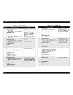
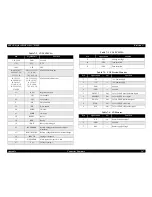
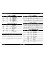
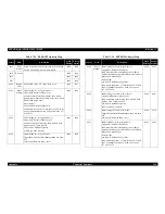
Table 7-2. CN1 PCMCIA
Pin
Signal name
Function
1,34,35,68
GND
Ground
17,51
VCC
VCC
18,52
VPP
VPP
41,40,39,38,37,
66,65,64,7,5,4,
3,2,32,31,30
CD15,14,13,12,
11,10,9,8,
7,6,5,4,3,2,1,0
PCMCIA slot data bus
56,55,54,53,
50,49,48,47,46,
19,20,14,13,
21,10,8,11,12,
22,23,24,25,26,
27,28,29
CA25,24,23,22,
21,20,19,18,17,
16,15,14,13,
12,11,10,9,8,
7,6,5,4,3,2,1,0
PCMCIA slot address bus
61
/REG
Register selection
7
/CE1
Card enable
42
/CE2
Card enable
9
/OE
Output enable
15
/WE
Write enable
44
/IORD
I/O read
45
/IOWR
I/O write
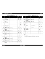
58
RESET
Reset
16
RDY
Ready
59
/WAIT
Bus cycle prolonged
62
BVD2/SPKR
Battery voltage detection/Audio digital
waveform
63
BVD1/STSCHG
Battery voltage detection/Card status change
60
INPACK
Input port response
33
WP/IOIS16B
Write protect/I/O port is 16 bits
43
VS1
Voltage sensing 1
57
VS2
Voltage sensing 2
36
/CD1
Card detection
67
/CD2
Card detection
Table 7-3. CN2 Preview Monitor
Pin
Signal name
I/O
Function
1
+5V
---
+5V power supply
2
+5V
---
+5V power supply
3
GND
---
Ground
4
GND
---
Ground
5
DETECT
Out
Color LCD I/F panel detection signal
6
XPNLRST
Out
Color LCD I/F reset signal
7
SDATA
Out
Color LCD I/F indication signal
8
SCLK
Out
Color LCD I/F shift clock
9
SCE
Out
Color LCD I/F chip enable signal
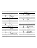
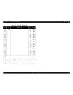
Table 7-4. CN4 Sensor
Pin
Signal name
I/O
Function
1
HP
In
Sensor detection signal
2
GND
---
Ground
3
HPV
---
Sensor supply voltage
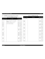
Table 7-2. CN1 PCMCIA
Pin
Signal name
Function


