background image


/Kits/1296-144CK.doc   


   8/15/2011


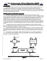
7.  Attach the PCB to the pallet.  Use two 4-40 x 3/16” screws by the antenna connector and 

two 4-40 x 1/4 screws with #4 flat washers by the oscillator section.  If you find solder interference 
between the PCB and the pallet, remove it by wicking or filing! 
 

8.  Attach the connector panel to the pallet.  Review the configurations below.  Your panel 

has all of the holes in it.  You may install all of the connectors or just the connectors you desire.  
Trim the Teflon on the connectors flush with the panel.  Use the 3-48 screws for the SMA 
connectors or 4-40 screws for the N connector.  The longer 3/8” screws go through the connector 
and panel, then into the pallet.  The short 3/16” screws hold the connectors to the panel.  You may 
use the screws to plug the holes if you do not use the connector.  After the connectors are 
installed, verify that the panel is a flush mount with the pallet and then solder the pins. If you need 
to re-position the PCB for the panel to be flush, do so. 


9. 


Use the bottom side component placement as a guide and wire the connections with the 

supplied #24 Teflon wire.  Install them all as shown. The connection from the +13 VDC connection 
and the RCA connector is done with the heavier green wire.  Make the connection from the PTT 
connector to the PCB. Install the ground lugs as shown with the short 1/8” 4-40 screws and solder 
the 1000 

ρ

F caps in place. 


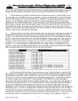
10.  Find the bottom half of the enclosure (the one with the holes in it) and line up the pallet 

with the mounting holes.  Insert any two 4-40 x 7/16” screws and start them. Install 2 flat head 
screws in the rear panel.  Be sure the wires are clear of the ribs and filters and tighten all screws.  
If the pallet wobbles, something is being pinched!!  Insert the switch into its position but do not 
solder.  Install the switch panel with 2 flat head screws then solder the exposed leads of the 
switch.  Install the LED’s.  The short lead is ground.  Now remove the pallet from the enclosure 
and trim all excess leads from the bottom side of the PCB and solder the mounting leads of the 
switch. 
 

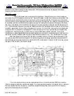
11.  Attach the M67715 to the pallet.  Use the thermal compound supplied, line up the pins 

with the PCB and use the 4-40 x 1/4 “ screws.  Solder the 5 pins.  Now make a determination of 
what keying scheme you will use, PTT-H (+ voltage) or PTT-L (Ground to transmit) and make the 
appropriate jumper connection from the PTT connection on the top side of the PCB. 
 

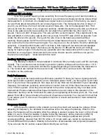
12.  Using the matrix below, make a determination of the required IF drive level and decide 

if you want a common or split IF.  All IF drive levels may be achieved from 1 mW to 10 watts by 
following the supplied schematic, matrix, and simplified component layout.  The 50 ohm load  
(R36) is mounted on the front panel and is installed after the pallet is aligned with the front panel 
during final test.   
 

13.  Install the IF coax between the IF connector (s) on the rear panel and their proper 

locations on the PCB. Refer to the custom pictorial for the correct configurations.   

Summary of Contents for 1296-144 CK

Page 1: ...relay on the RF side with provisions for external switching for adding a high power amplifier or preamplifier to your 23 cm system The 144 MHz IF levels and options are adjustable on both transmit and...

Page 2: ...le helical filter that allows approximately 30 MHz of amplified bandwidth This signal is then amplified by a high level MMIC before being filtered by the next 3 pole helical filter that restricts the...

Page 3: ...t a small tool such as a small bladed screw driver can be used to flatten them before attempting to solder See Figure 2 After verifying that the leads are flat to the surface you will be ready to sold...

Page 4: ...ly As an alternate method you can insert one component at a time in the correct mounting location and gently push down to the circuit board while holding the component flip over the circuit board and...

Page 5: ...ist Bag 1 Bag 4 Each side of the printed circuit board PCB is also shown to eliminate mirror image assembly errors The top and bottom side assembly operation should always begin by aligning the PCB ou...

Page 6: ...de of the circuit board per the top side component placement diagram Do not install IC4 VR1 VR4 or D1 D9 3 Install all surface mount capacitors and resistors and L31 per the topside component placemen...

Page 7: ...place 10 Find the bottom half of the enclosure the one with the holes in it and line up the pallet with the mounting holes Insert any two 4 40 x 7 16 screws and start them Install 2 flat head screws i...

Page 8: ...Installed IF Connections Common or Split Start the Testing Procedure 1 All of the initial testing of the transverter is done with the pallet assembly only Before you start verify that all components...

Page 9: ...ve the mentioned test equipment install the mixer after verification of the RX voltages If you have an mW meter connect a coax pigtail to the open pad on C17 This will be the LO circuit s output and t...

Page 10: ...ge is out of tolerance verify all surrounding components and recheck bottom side wiring Remember MMICs draw a specified amount of current but may be a bit out of tolerance LOCATION TX VOLTAGE Matrix r...

Page 11: ...high in frequency or to low If it is to high remove the LO shield and compress the L1 inductor and readjust C2 If the frequency is to low spread the coil slightly and re adjust C2 If the frequency is...

Page 12: ...a non hostile RF environment If your LNA is a ultra low noise unit it most likely will not have the IP3 performance the transverter has It will overload before any component in the transverter will So...

Page 13: ...pen and NC normally closed The C connection can be wired to ground or positive voltage such as the source 13 8 VDC The K2 common connection will then be toggled depending on what state the transverter...

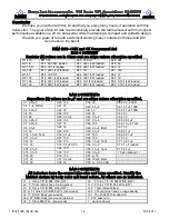
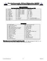
Page 14: ...fied C1 0 01 F C20 100 C39 33 C60 0 3 3 VAR C2 1 4 Piston C21 18 C40 0 1 F C61 0 1 F 1008 C3 0 01 F C23 18 C41 33 C62 0 1 F 1008 C4 18 C24 100 C42 33 C63 33 C5 22 C25 0 01 F C43 0 1 F C64 33 C6 0 01 F...

Page 15: ...HC 18 U D8 1N914 HARDWARE 2 1000 F leaded R36 THC 50 10 W Load 1 Type N connector SW1 Power Switch 2 SMA connectors 1 Shield Prepped 2 BNC Female UG1094 U Connectors 3 18 Teflon wire 3 RCA Jacks Contr...

Page 16: ......

Page 17: ...o o o o o o o r o o o o o o o o o BB 6 6 o RR 5 5 o o o o o o o o o o o o o o O u ololo l n l i a l f lYto I Xlrxo o o l L l ooo t o o o o o o o o o o o o o P lo o t l Fc 1 of AS o o o o o ol S o o x...

Page 18: ...o o o o o o o ru LN o o C o o 1 d o o o J T X L o o o L l k l o o a n 1 l v ff t o o o o 0 e 1Jfl L4 lo o o e s i o 1T I l to3 alf llll UdC AlEl l SSU 99 U b F I q6 _ I 1 Y o o o O O o o o o o o o l...

Reviews: