background image


/Kits/1296-144CK.doc   


   8/15/2011


Soldering surface mounted passive components such as chip resistors and capacitors: 

1.  Determine the component mounting position based on the assembly diagram.  
2.  Without the component, tin one of the mounting pads not shared by another component. 
(Flow a small amount of solder on it) 
3.  After cooling, place the component in the correct position per the assembly diagram, it 
should now have one end over the tinned area. 
4.  Holding the component in place with tweezers or other soldering aid, heat the tinned area 
and allow the solder to flow around the component. Remove the heat. 
5.  Once solidified, remove holding tool and heat and flow solder to the other side of the 
component only if it is not shared by a second component. If so, solder the component that 
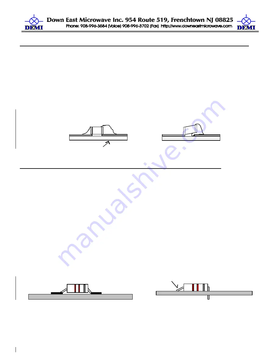
shares the pad first.  You are done!  See examples in figure 3. 

Circuit board

Correct

Incorrect

Solder Fillet

Incorrect Component

Placement


Figure 3. Proper SMD Assembly.


Soldering leaded components (resistors, capacitors, diodes, and inductors) : 
 

Depending on your available tools, you can solder your transverter's leaded components 

from either the top or bottom of the PCB.  It is suggested for the home assembler to use a method 
that is comfortable.  A simple holding vise can be utilized to allow the components to be 'dropped 
in' from the top side and soldered on this side without flipping over the assembly.  As an alternate 
method, you can insert one component at a time in the correct mounting location and gently push 
down to the circuit board, while holding the component, flip over the circuit board and bend the 
leads over in opposite direction to hold the component in place.  Although this is the most reliable 
method, there are some drawbacks if the component must be removed when the PCB is installed 
in the enclosure. 
 

Some leaded components may need to be surfaced mounted either on one or more leads.  

If this is the case, the leads need to be pre-formed before soldering.  If you see a leaded 
component on the component placement diagram without a circle at the end of the lead such as 
R25 and C49, those leads will need to be surfaced mounted as shown in the drawings below. DO 
NOT install any leaded components in the ground via holes if it is shown as a surface mount lead. 
The PCB mounts to a pallet and if there is any solder or extended lead interference, the PCB will 
not be flush with the pallet.  


Leads soldered to PCB surface 

Circuit Board Surface 


This end soldered to PCB surface 

Circuit Board Surface 


Figure 4


Some inductors are pre-formed and some will need to be formed such as L1. It is 

suggested that the coils be formed on the supplied wooden dowel. Winding coils is not an exact 
science and you should not be intimidated by it.  Using the enamel wire supplied, extend about ¼" 
in a perpendicular direction off of the dowel and wind the wire around it, counting each revolution 
as one turn.  When the total number of turns is completed (see the component list) cut the wire an 

Summary of Contents for 1296-144 CK

Page 1: ...relay on the RF side with provisions for external switching for adding a high power amplifier or preamplifier to your 23 cm system The 144 MHz IF levels and options are adjustable on both transmit and...

Page 2: ...le helical filter that allows approximately 30 MHz of amplified bandwidth This signal is then amplified by a high level MMIC before being filtered by the next 3 pole helical filter that restricts the...

Page 3: ...t a small tool such as a small bladed screw driver can be used to flatten them before attempting to solder See Figure 2 After verifying that the leads are flat to the surface you will be ready to sold...

Page 4: ...ly As an alternate method you can insert one component at a time in the correct mounting location and gently push down to the circuit board while holding the component flip over the circuit board and...

Page 5: ...ist Bag 1 Bag 4 Each side of the printed circuit board PCB is also shown to eliminate mirror image assembly errors The top and bottom side assembly operation should always begin by aligning the PCB ou...

Page 6: ...de of the circuit board per the top side component placement diagram Do not install IC4 VR1 VR4 or D1 D9 3 Install all surface mount capacitors and resistors and L31 per the topside component placemen...

Page 7: ...place 10 Find the bottom half of the enclosure the one with the holes in it and line up the pallet with the mounting holes Insert any two 4 40 x 7 16 screws and start them Install 2 flat head screws i...

Page 8: ...Installed IF Connections Common or Split Start the Testing Procedure 1 All of the initial testing of the transverter is done with the pallet assembly only Before you start verify that all components...

Page 9: ...ve the mentioned test equipment install the mixer after verification of the RX voltages If you have an mW meter connect a coax pigtail to the open pad on C17 This will be the LO circuit s output and t...

Page 10: ...ge is out of tolerance verify all surrounding components and recheck bottom side wiring Remember MMICs draw a specified amount of current but may be a bit out of tolerance LOCATION TX VOLTAGE Matrix r...

Page 11: ...high in frequency or to low If it is to high remove the LO shield and compress the L1 inductor and readjust C2 If the frequency is to low spread the coil slightly and re adjust C2 If the frequency is...

Page 12: ...a non hostile RF environment If your LNA is a ultra low noise unit it most likely will not have the IP3 performance the transverter has It will overload before any component in the transverter will So...

Page 13: ...pen and NC normally closed The C connection can be wired to ground or positive voltage such as the source 13 8 VDC The K2 common connection will then be toggled depending on what state the transverter...

Page 14: ...fied C1 0 01 F C20 100 C39 33 C60 0 3 3 VAR C2 1 4 Piston C21 18 C40 0 1 F C61 0 1 F 1008 C3 0 01 F C23 18 C41 33 C62 0 1 F 1008 C4 18 C24 100 C42 33 C63 33 C5 22 C25 0 01 F C43 0 1 F C64 33 C6 0 01 F...

Page 15: ...HC 18 U D8 1N914 HARDWARE 2 1000 F leaded R36 THC 50 10 W Load 1 Type N connector SW1 Power Switch 2 SMA connectors 1 Shield Prepped 2 BNC Female UG1094 U Connectors 3 18 Teflon wire 3 RCA Jacks Contr...

Page 16: ......

Page 17: ...o o o o o o o r o o o o o o o o o BB 6 6 o RR 5 5 o o o o o o o o o o o o o o O u ololo l n l i a l f lYto I Xlrxo o o l L l ooo t o o o o o o o o o o o o o P lo o t l Fc 1 of AS o o o o o ol S o o x...

Page 18: ...o o o o o o o ru LN o o C o o 1 d o o o J T X L o o o L l k l o o a n 1 l v ff t o o o o 0 e 1Jfl L4 lo o o e s i o 1T I l to3 alf llll UdC AlEl l SSU 99 U b F I q6 _ I 1 Y o o o O O o o o o o o o l...

Reviews: