BGS3 Hardware Interface Description
4.2 RF Line Routing Design
67
BGS3_HD_v01.000d
Page 65 of 109
2010-03-26
Confidential / Released
Note: As shown in
the ground copper area between the antenna RF_OUT pad and
the side of the module is slightly carved. This area should be used for the antenna line.
To prevent receiver desensitization due to interferences from components on the application
PCB, the antenna connection line should be shielded, using Stripline technology rather than
Microstrip. Please see
for an example of how to design the antenna connection in
order to achieve the required 50
Ω
line impedance.
For type approval purposes, the module can be equipped with an optional coaxial antenna con-
nector (U.FL-R-SMT) along with other necessary components. The U.FL-R-SMT connector
has been chosen as antenna reference point (ARP) for the Cinterion Wireless Modules refer-
ence equipment submitted to type approve BGS3. All RF data specified throughout this docu-
ment is related to the ARP.
Due to the immediate vicinity of both, the ARP and the antenna pad, no differences in the RF
parameters are expected.
4.2
RF Line Routing Design
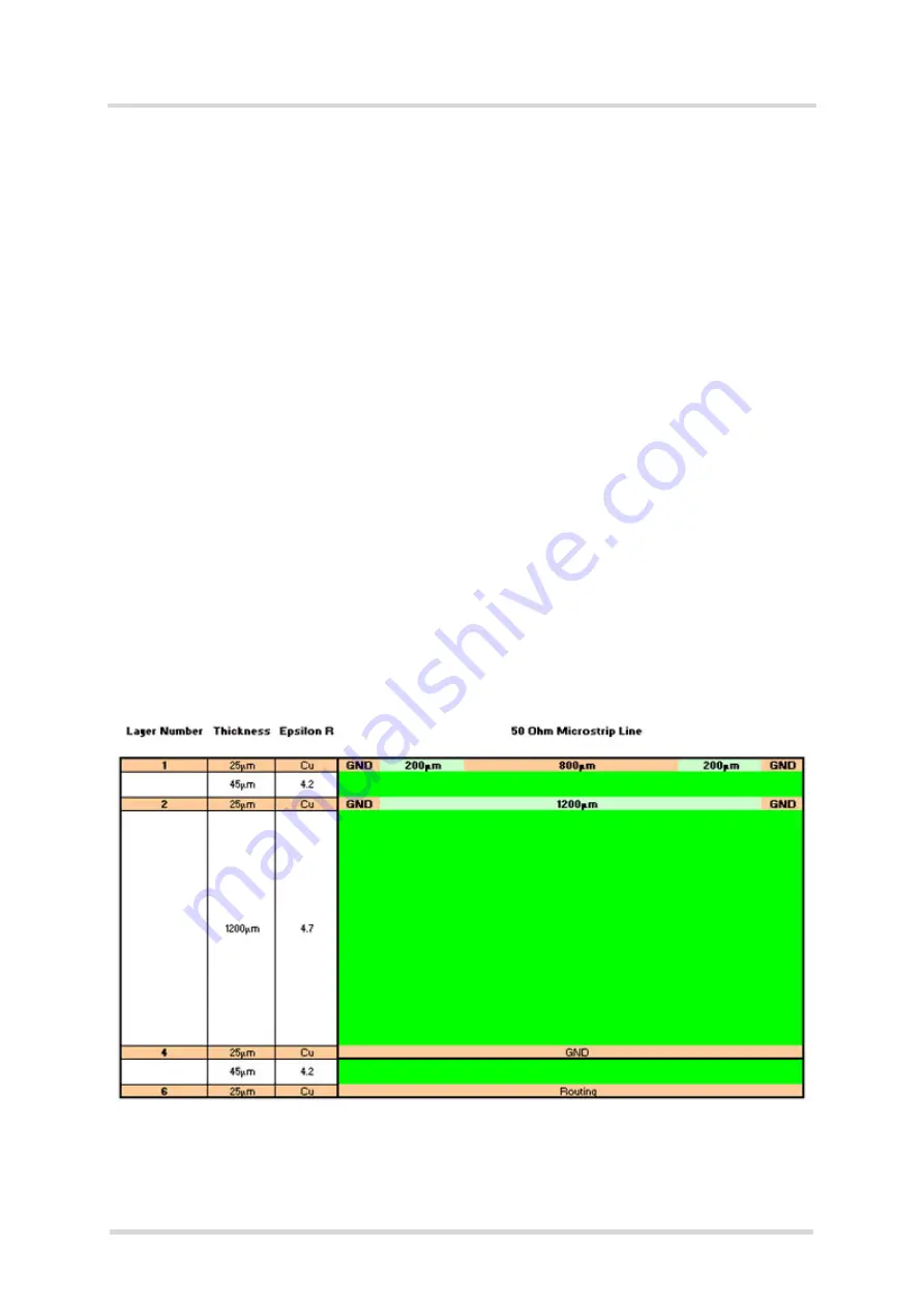
To give an example, Cinterion has developed an interface adapter board for EGS3 that gives
a hint of how an application board could be designed with respect to the correct RF line imped-
ance.
The interface board has a 4 layer PCB stack - as shown in
.
Figure 31:
4 layer PCB stack for BGS3 interface board


