


MC97F6108A User’s manual
20. Electrical characteristics
231
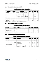
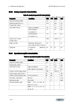
20.18
Internal Flash ROM characteristics
Table 55. Internal Flash ROM Characteristics
(T
A
=-40°C ~ +85°C, VDD=2.7V ~ 5.5V, VSS= 0V)
Parameter
Symbol
Condition
MIN
TYP
MAX
Unit
Sector write time
t
FSW
–
–
2.5
2.7
ms
Sector erase time
t
FSE
–
–
2.5
2.7
Code write protection time
t
FHL
–
–
2.5
2.7
Page buffer reset time
t
FBR
–
–
–
5
us
Flash programming frequency
f
PGM
–
0.4
–
–
MHz
Endurance of Write/Erase
NF
WE
–
–
–
10,000 times
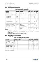
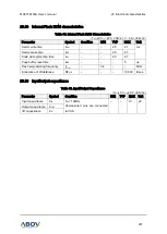
20.19
Input/output capacitance
Table 56. Input/Output Capacitance
(T
A
=-40°C ~ +85°C, VDD=0V)
Parameter
Symbol
Condition
MIN TYP MAX Unit
Input capacitance
C
IN
f
IRC
= 16MHz
Unmeasured pins are connected
to VSS
–
–
10
pF
Output capacitance C
OUT
I/O capacitance
C
IO