


MC97F6108A User’s manual
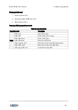
19. Memory programming
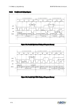
201
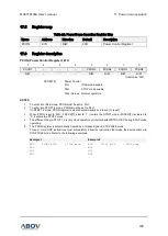
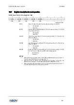
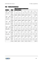
FECR (Flash Control Register): EBH
7
6
5
4
3
2
1
0
AEF
-
EXIT1
EXIT0
WRITE
READ
nFERST
nPBRST
R/W
-
R/W
R/W
R/W
R/W
R/W
R/W
Initial value: 03H
AEF
Enable Flash bulk erase mode
0
Disable bulk erase mode of Flash memory
1
Enable bulk erase mode of Flash memory
EXIT[1:0]
Exit from program mode. It is cleared automatically after 1 clock
EXIT1
EXIT0
Description
0
0
Don’t exit from program mode
0
1
Don’t exit from program mode
1
0
Don’t exit from program mode
1
1
Exit from program mode
WRITE
Start to program or erase of Flash. It is cleared automatically after 1 clock
0
No operation
1
Start to program or erase of Flash
READ
Start auto-verify of Flash. It is cleared automatically after 1 clock
0
No operation
1
Start auto-verify of Flash
nFERST
Reset Flash control logic. It is set automatically after 1 clock
0
Reset Flash control logic
1
No operation (default)
nPBRST
Reset page buffer with PBUFF. It is set automatically after 1 clock
PBUFF
nPBRST
Description
0
0
Page buffer reset
1
0
Page buffer select register reset
X
1
No operation (default)
NOTE
: WRITE and READ bits can be used in program, erase and verify mode with FEAR
registers. Read or writes for memory cell or page buffer uses read and write enable
signals from memory controller. Indirect address mode with FEAR is only allowed to
program, erase and verify