


FM680 User Manual
r1.7
FM680
Page 27 of 32
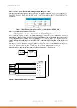
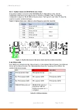
Virtex-5
(FPGA_A)
Virtex 6
(FPGA_B)
CPLD
125 MHz
16 MHz
T6
AE30/AF30
W30/V30
Y30
AA31
P8/P7
Y2
Y3
CDCM1804
CDCE925
Y0
Y1
Y1
Y4
Y5
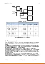
Figure 11 : Clock tree
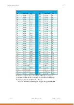
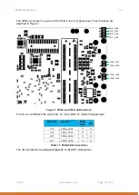
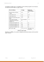
FPGA Pin
Net Name
DIR
CDCE925, CDCV1804
Device
Pin Number
Pin Name
V5_T6
CLK_SYNTH_A
I
CDCE925
13
Y1
V6_Y30
CLK_SYNTH_B
I
CDCE925
7
Y4
V6_AA31
CLK_SYNTH_B
I
CDCE925
8
Y5
V5_P7
CLK125_AN
I
CDCV1804
10
Y2-
V5_P8
CLK125_AP
CDCV1804
9
Y2+
V6_V30
CLK125_B0N
I
CDCV1804
16
Y0-
V6_W30
CLK125_B0P
CDCV1804
15
Y0+
V6_AF30
CLK125_B1N
I
CDCV1804
22
Y1-
V6_AE30
CLK125_B1P
CDCV1804
21
Y1+
Table 21: Miscellaneous clock connections
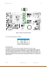
6 Power requirements
The Power is supplied to the FM680 via the XMC Pn5 connector. Several DC-DC converters
generate the appropriate voltage rails for the different devices and interfaces present on
board.
The FM680 power consumption depends mainly on the FPGA devices work load. By using
high efficiency power converters, all care has been taken to ensure that power consumption
will remain as low as possible for any given algorithm.
After power up, the FM680 typically consumes 6 Watts of power. For precise power
measurements it is recommended to use the Xilinx power estimation tools for both the Virtex-
5 and Virtex-6 FPGA devices. The maximum current rating given in the table below is the
maximum current that can be drawn from each voltage rail in the case resources are used to
their maximum level.
Special precautions need to be taken to support the XMC VPOWER input, since the XMC
standard dictates that this power supply can either be 12V or 5V. To overcome this, a voltage
detection circuit detects whether VPOWER is 12V or 5V and enables a switching regulator or


