FM680 User Manual
r1.7
FM680
Page 19 of 32
5.9.2 Power connection to the front panel I/O daughter card
The Front Panel I/O daughter card on side 1 of the PCB is powered via a 7-pin connector of
type BKS (Samtec). Each pin can carry up to 1.5A. The power connector’s pin assignment is
as follows.
Pin #
Signal
Signal
Pin #
1
+3.3V
+3.3V
2
3
+5V
GND
4
5
+12V
GND
6
7
-12V
Table 13: Daughter card power connector pin assignment on PMC side 1
5.9.3 Front Panel optical transceivers
(Special build option and not in combination with the front panel daughter card)
Four 2.5 GB/s optical transceivers (LTP-ST11M) are available on the FM680 in the front
panel area. They are connected to the MGT I/Os of the Virtex-6. Infiniband protocols as well
as Gigabit Ethernet and Fibre channel (sFPDP) can be implemented over the transceivers.
Lower rate optical transceivers (2.125 GB/s and 1.0625 GB/s) are available in the same form
factor.
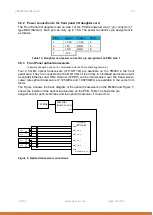
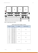
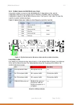
The Figure 4 shows the block diagram of the optical transceivers on the FM680 and Figure 5
shows the location of the optical transceivers on the PCB. Table 14 shows the pin
assignments for each serial lane and the optical transceiver it connects to.
Clk buffer
(874003BG-05LF)
125 MHz
OT3
TX
RX
MGT_116_3
Virtex 6
(FPGA B)
OT2
TX
RX
MGT_116_2
OT1
TX
RX
MGT_116_1
OT0
TX
RX
MGT_116_0
MGTREFCLK_116_0
QA0
en
en
en
en
AB31
AA30
Figure 4: Optical transceiver connections


