FM680 User Manual
r1.7
FM680
Page 26 of 32
3
2
1
6
5
4
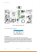
VCC
GND
TCK
TMS
TDI
TDO
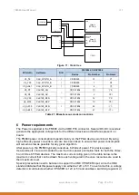
Figure 10: JTAG connector (J6) location
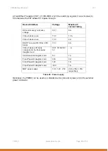
The JTAG connector pinout is as follows:
Pin #
Signal Signal Pin #
1
1.8V
TMS
4
2
GND
TDI
5
3
TCK
TDO
6
Table 20 : JTAG pin assignment
5.12 Clock tree
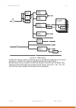
The FM680 clock architecture offers an efficient distribution of low jitter clocks.
Both FPGA devices receive a low jitter 125MHz clock. A low jitter programmable clock able
to generate frequencies from 62.5MHz to 255.5MHz in steps of 0.5MHz is also available.
This clock management approach ensures maximum flexibility to efficiently implement multi-
clock domains algorithms and use the memory devices at different frequencies. Both clock
buffer devices (CDCV1804) and the frequency synthesizer (CDCE925) are controlled by the
Virtex-5 device.


