FM680 User Manual
r1.7
FM680
Page 23 of 32
5.11 FPGA configuration
5.11.1 Flash storage
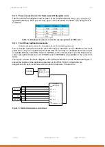
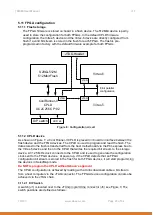
The FPGA firmware is stored on board in a flash device. The 512Mbit device is partly
used to store the configuration for both FPGAs. In the default CPLD firmware
configuration, the Virtex-5 device and the Virtex-6 device are directly configured from
flash if a valid bit stream is stored in the flash for each FPGA. The flash is pre-
programmed in factory with the default firmware example for both FPGAs.
CoolRunner-II
CPLD
XC2C256 CP132
S29GL512M
512Mbit Flash
Virtex-6
Virtex-5
JTAG Header
JTAG
JTAG
JTAG
LED x4
DIP switch
8-bit parallel
configuration
Figure 8 : Configuration circuit
5.11.2 CPLD device
As shown on Figure 7, a Cool Runner-II CPLD is present on board to interface between the
flash device and the FPGA devices. The CPLD is used to program and read the flash. The
data stored in the flash is transferred from the host motherboard via the PCI-express bus to
the Virtex-5 device and then to the CPLD that writes the required bit stream to the storage
device. A 31.25 MHz clock connects to the CPLD and is used to generate the configuration
clock sent to the FPGA devices. At power up, if the CPLD detects that an FPGA
configuration bit stream is stored in the flash for both FPGA devices, it will start programming
the devices in SelecMap mode.
Do NOT reprogram the CPLD without Abaco’s approval
The CPLD configuration is achieved by loading with a Xilinx download cable a bit stream
from a host computer via the JTAG connector. The FPGA devices configuration can also be
achieved via the JTAG chain.
5.11.2.1 DIP Switch
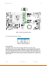
A switch (J1) is located next to the JTAG programming connector (J6) see Figure 9. The
switch positions are defined as follows:


