


FM680 User Manual
r1.7
FM680
Page 25 of 32
OFF
ON
FLASHING
LED 0
(red)
FPGA A configured
FPGA A not configured
FPGA A or B bit stream or
user_ROM_register is
currently being written to the
flash
LED 1
(red)
FPGA B configured
FPGA B not configured
FPGA A or B bit stream or
user_ROM_register is
currently being written to the
flash
LED 2
(red)
FLASH idle
FLASH busy
Safety configuration loaded
into FPGA A, or attempted to
load.
LED 3
(red)
No CRC error detected
CRC error. Presumably a
wrong or corrupted FPGA bit
stream has been written to
the flash. Once on this LED
remains on
n.a.
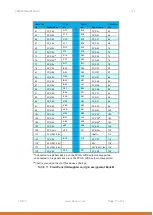
Table 19: LED board status
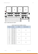
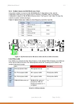
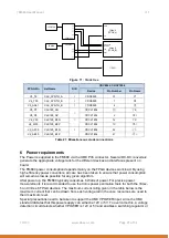
The LEDs are located on side 2 of the PCB in the front panel area. Their locations are
depicted in Figure 7.
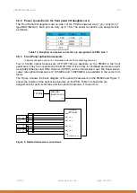
5.11.3 JTAG
A JTAG connector is available on the FM680 for configuration purposes. The JTAG can also
be used to debug the FPGA design with the Xilinx Chipscope. A press fit connector is
delivered with the board that can be plugged into the connector holes.
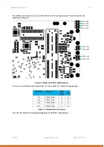
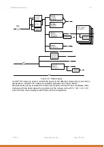
The JTAG connector can be placed on both sides of the PCB. The connector location seen
from the bottom of the PCB is shown in Figure 10.


