44
Virtex-6 FPGA System Monitor
UG370 (v1.1) June 14, 2010
Analog Inputs
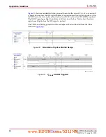
The bipolar input mode also accommodates inputs signals driven from a true differential
source for example, a balanced bridge. In this case, V
N
and V
P
can swing positive and
negative relative to a common mode or reference voltage (see
). The maximum
differential input (V
P
– V
N
) is ±0.5V. With maximum differential input voltages of ±0.5V
and assuming balanced inputs on V
N
and V
P
,the common mode voltage must lie in the
range 0.25V to 0.75V.
The output coding of the ADC in bipolar mode is two’s complement and is intended to
indicate the sign of the input signal on V
P
relative to V
N
. The designed code transitions
occur at successive integer LSB values that is, 1 LSB, 2 LSBs, 3 LSBs etc. The LSB size in
volts is equal to 1V/2
10
or 1V/1024 = 0.977 mV. The ideal transfer function is illustrated in
X-Ref Target - Figure 22
Figure 22:
Bipolar Signals
X-Ref Target - Figure 23
Figure 23:
Bipolar Transfer Function
UG
3
70_22_060
8
09
V
P
V
CM
=
(V
P
+
V
N
) / 2
V
P
, V
N
Vo
lt
s
V
N
0V
0.5V
1.5V
2.5V
1V
2V
Common Mode R
a
nge
0.25V to 0.75V
V
P
V
N
Common
Volt
a
ge
0.25V to 0.75V
±0.25V
+
+
±0.25V
ADC
Output Code
(Two’s Complement
Coding)
-3
+1 +2
0
-2 -1
+499
-500
Full Scale Input = 1V
1 LSB = 1V / 1024 = 0.977 µV
200h
201h
000h
001h
002h
1FEh
1FFh
3FFh
3FEh
3FDh
10-Bit Output Code
Input Voltage (mV)
UG370_23_060809
www.BDTIC.com/XILINX


