


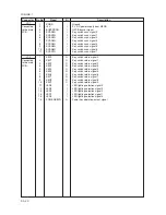


2DA/2DB-1
2-3-21
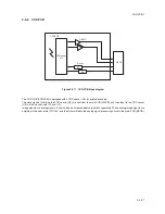
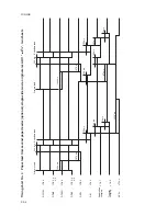
Figure 2-3-11 CCD PCB block diagram
The CCD PCB (CCDPCB) is equipped with a CCD sensor (U2) for original scanning.
The clock signals for driving the CCD sensor (U2) are sent from the main PCB (MPCB), and then input to the CCD sensor
(U2) via the clock drivers (U1 and U3).
Image signals are analog signals. Even- and odd-numbered pixels are output separately. These analog image signals are
amplified in the transistors (TR1 to 4) and then transmitted to the analog signal processing circuit in the main PCB (MPCB).
2-3-6
CCD PCB
MPCB
Tr.AMP
Driver
CCD sensor
U2
U1
U3
CCDPCB
Содержание cd 1116
Страница 1: ...Service Manual Copy CD 1116 CD 1120 Rev 1 ...
Страница 2: ...Service Manual Copy DC 2116 DC 2120 Rev 1 ...
Страница 4: ...This page is intentionally left blank ...
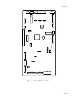
Страница 247: ...2DA 2DB 1 2 3 2 Figure 2 3 2 Power source PCB silk screen diagram 220 240 V AC 120 V AC ...
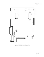
Страница 264: ...2DA 2DB 1 2 3 19 Figure 2 3 10 Operation unit PCB silk screen diagram ...


